A microstrip gap waveguide is simulated over a mushroom-type electronic band gap (EBG) surface to demonstrate the effectiveness of the design. The simulations shown in this example are taken from a design in the referenced paper [1].
The device operates in the 5-12 GHz range and consists of a mushroom-type EBG substrate with a trace inserted between two walls. The entire device is enclosed in a metal box with the only openings the two ports at each end. Views of the geometry in CAD format are shown in Figures 1 and 2 where the top of the box has been made invisible to show the interior details. The device is designed so that propagation takes place in the air region between the mushrooms and the top of the box. As the width of the air region is only one millimeter, a fairly small FDTD mesh size of 0.2 mm is used to provide enough resolution for the fields. A three-dimensional view of the mesh near one of the ports is shown in Figure 3 where the display of the metal box and the dielectric substrate is disabled to show the details. The XACT meshing feature is used for the EBG and microstrip parts of the geometry to accurately mesh the curves and edges.
Figure 1: A CAD rendering of the geometry shown from the top. Here the lid of the metal box containing the device has been removed to reveal the contents of the interior.
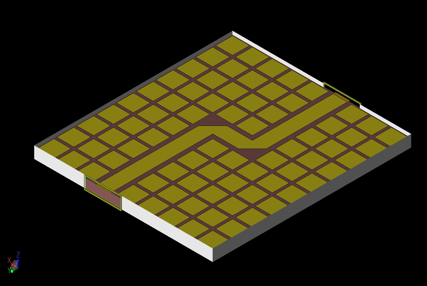
Figure 2: A CAD view of the geometry shown at an angle with the top of the box removed.
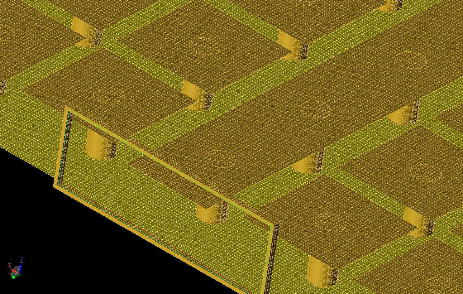
Figure 3: A three-dimensional view of the XFdtd mesh of the device near one of the ports. The box and substrate have been removed in this view to show the interior detail.
The device is excited by TEM waveguide ports attached to each end of the microstrip line. The excitation, shown in Figure 4, is applied with a frequency-limited signal with content from about 5 to 12 GHz to one of the ports. S-parameter and field image data is saved as output.
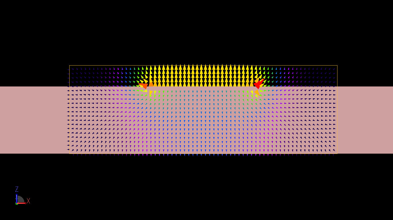
Figure 4: The field pattern of the input excitation at port 1 where the fields are shown to be primarily between the microstrip line and the metal cover.
The calculation is executed on an NVidia Tesla C1060 GPU card in approximately 39 minutes while using about 206 MB of memory. The calculation takes a fairly long time to converge due to resonant fields in the box which decay slowly.
Following the simulation, the computed S-parameters can be compared to measured data presented in the paper [1]. In Figures 5 and 6 the S11 and S21 results are plotted, respectively, against the measured data and show similar results. The steady state electric field distribution at 9 GHz in the middle of the air region above the EBG surface is plotted in Figure 7. Here it can be seen that the fields are contained in the region above the microstrip line as expected. Finally, the steady state conduction currents on the EBG surface are plotted at 9 GHz and are shown in Figure 8 and again the field strength can be seen to drop of significantly away from the microstrip line.
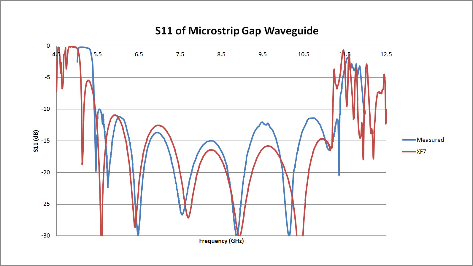
Figure 5: A comparison of the return loss (S11) of the device as simulated in XFdtd shown with measured data.
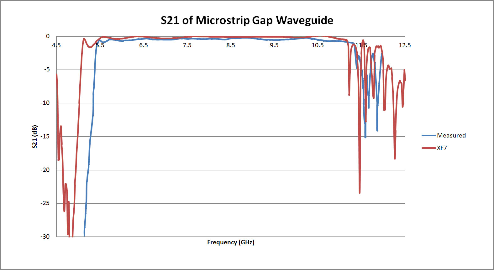
Figure 6: A comparison of S21 of the device between the simulated XFdtd results and measurements.
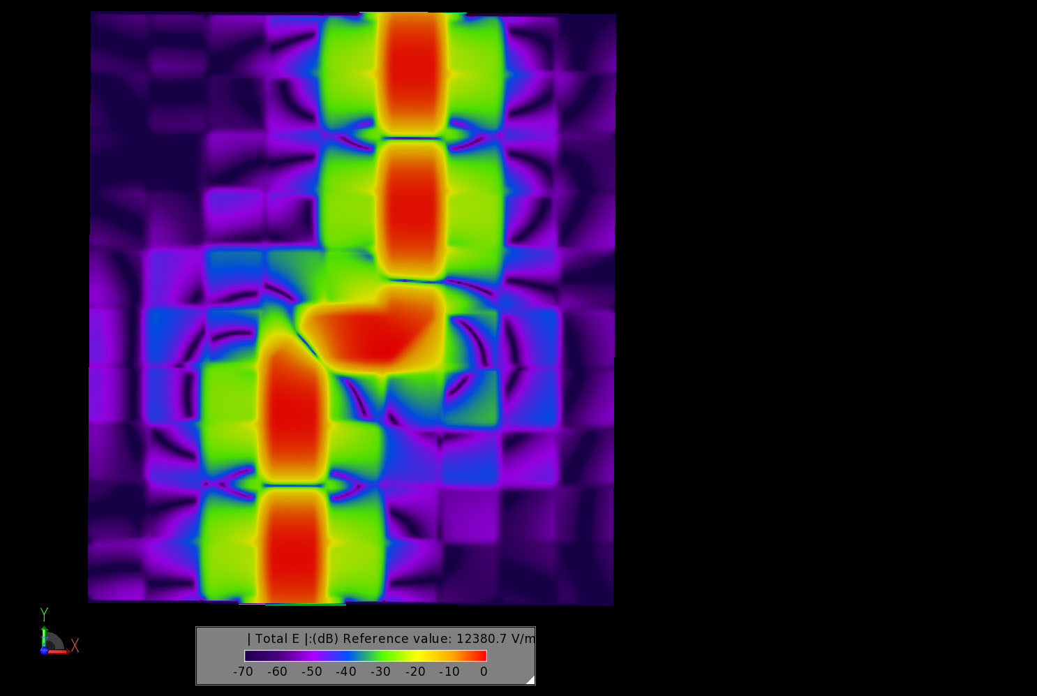
Figure 7: The steady state electric field distribution at 9 GHz in the center of the air region between the EBG surface and the metal lid of the box. The fields are shown to be tightly constrained to the microstrip region.
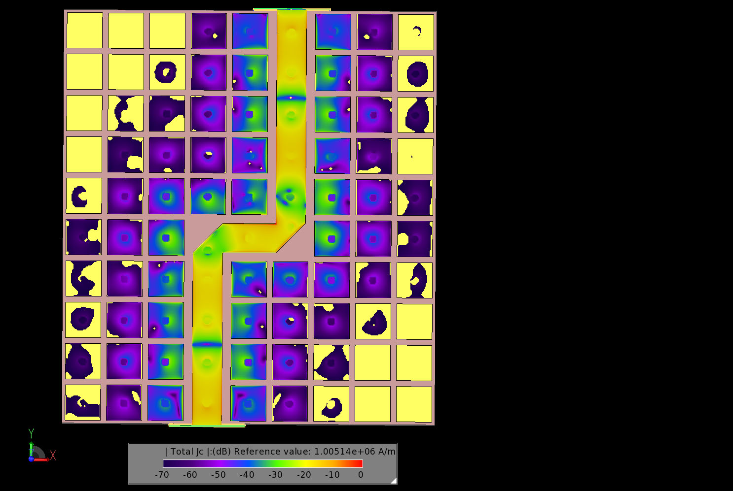
Figure 8: The steady state conduction currents on the top of the EBG surface. The currents are bound tightly to the microstrip region.
References
-
E. Pucci, E. Rajo-Iglesias, P. S. Kildal, “New Microstrip Gap Waveguide on Mushroom-Type EBG for Packaging of Microwave Components,” IEEE Microw. Wireless Compon. Letters, Vol. 22, No. 3, Mar. 2012, pp. 129-131.