The Rotman Lens Designer (RLD) software is a first-level tool for designing microstrip and stripline Rotman Lenses. The calculations in the tool are based on Geometrical Optics combined with the lens design equations developed by Rotman [1] and others [2]. The RLD software can rapidly produce a tuned lens design from a set of design parameters. The software was developed for use in the X band, but there is no inherent limitation in the software that prevents it from operating at much higher frequencies. This study will take a basic lens design and hold most design parameters constant while varying the center frequency and compare the results produced with those from a full wave solution derived by the XFdtd software.
A general set of lens design parameters are selected for the example. The first lens designed has a center frequency of 4.8 GHz and a bandwidth of 0.8 GHz. Other lenses tested will be multiples of these frequency values. The scan angle is 40 degrees with output element spacing of 0.46431 wavelengths (separation distance between the output array elements). The lens is constructed as a microstrip with a substrate material that will vary in thickness and material properties as the frequency changes. The number of beam and array ports will be fixed at 8 input and 8 output for all cases. In addition, for all cases the lens is tuned for good performance in the RLD software.
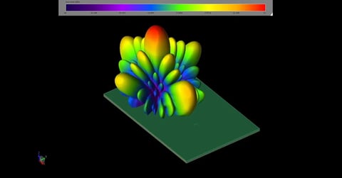
Figure 1 shows a basic 8x8 lens created by RLD with the beam ports to the left and the array ports to the right. On the top and bottom are dummy ports attached to the sidewalls that are intended to absorb any fields that strike them. The beam ports are numbered 1 to 8 from bottom to top. When the bottom port (Beam 1) is active, it will produce a beam centered at the positive maximum scan angle. A beam near the center, for example Beam 4, will produce a beam that is closer to broadside of the array. The top port (Beam 8) will produce a beam at the negative maximum scan angle. Figure 2 shows the 8 beams produced by the lens of Figure 1 with Beam 1 at the far right and Beam 8 at the far left.
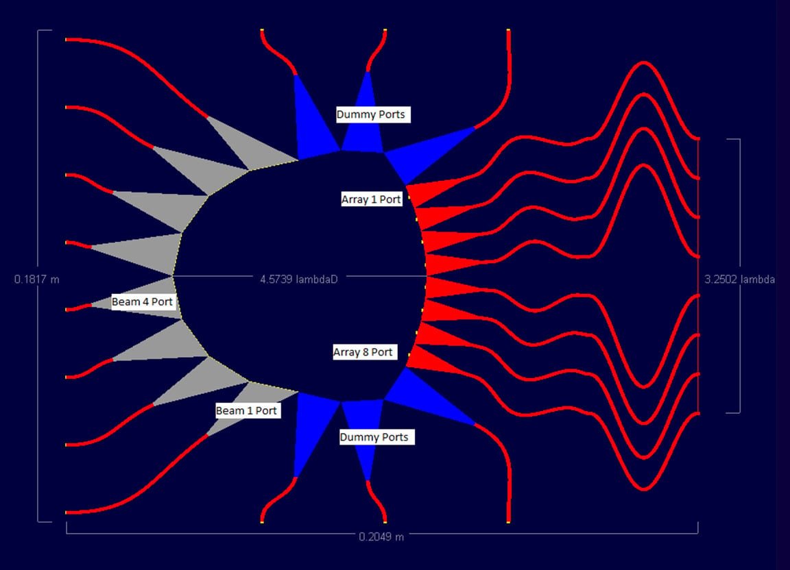
Figure 1: Shown is a basic microstrip lens generated in the RLD software. To the left are the beam (input) ports and to the right are the array (output ports). The port numbering is identified in the figure. The blue ports at the top and bottom are the dummy ports on the sidewalls. This example will vary the curvature of the sidewall while holding other lens parameters fixed.
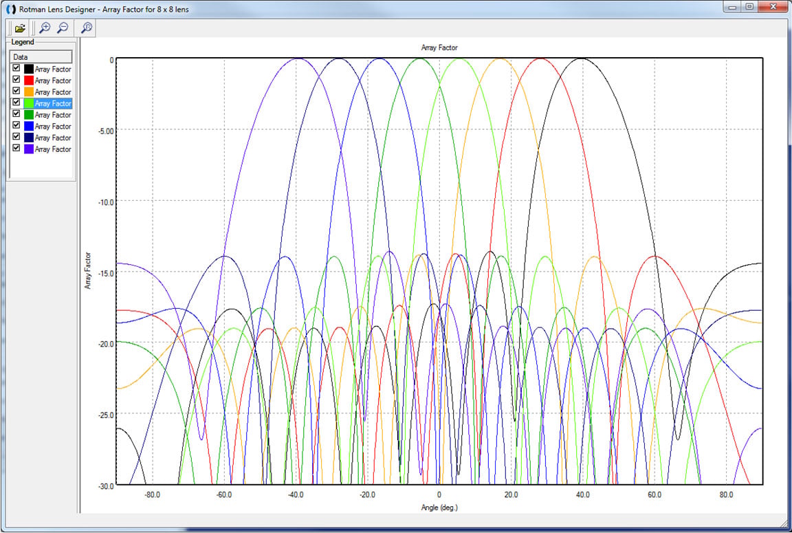
Figure 2: This is a plot of the 8 beams produced by the lens of Figure 1 in the RLD software. The maximum scan angle of the beam is +/- 40 degrees which is generated by ports 1 and 8 on the input side
This example will vary the center frequency of the lens from 4.8 GHz up to 78.6 GHz. Most design parameters will remain constant but the dielectric substrate material selection will vary resulting in changes in the thickness and material properties of the dielectric. For most of the designs, a dielectric material with relative permittivity of 3.0 and loss tangent of 0.0013 is used. The substrate thickness of this material decreases as the frequency increases to maintain well-defined microstrip transmission lines with a 50 ohm impedance. At the highest frequency of 78.6 GHz, three different designs, each using a different dielectric material, are simulated to find the best practical design. The highest dielectric constant simulated is 11.20 with loss tangent of 0.0022. A third option uses a dielectric of 6.5 and loss tangent of 0.002. The point of the investigation is to verify that the results produced by RLD are a good match to those from a full wave solver for lenses with center frequencies that extend well beyond the X band.
At the low end of the frequency range of 4.8 GHz, the lens is fairly large at about 37 x 34 cm when using a substrate with a dielectric constant of 3.0.The substrate thickness is selected as 0.768 mm to provide well-defined transmission lines. A thinner substrate will give very thin lines that will be difficult to resolve in the software and are harder to fabricate while a thicker substrate will generate fatter lines that can make the layout difficult and cause some of the subtle curves in the line to disappear, making the electrical length of the lines incorrect. The chosen best-design lens is shown in Figure 3 as displayed in the RLD software. After simulation in both RLD and XFdtd, the array factor beam pattern is plotted and found to give a high correlation (greater than 95%) between the two software results. Figure 4 shows the pattern for Beam 1 while Figure 5 shows the pattern of Beam 4.
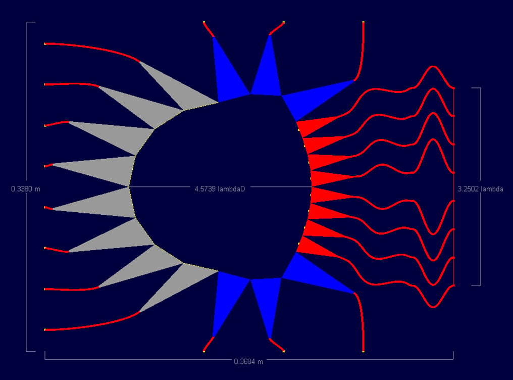
Figure 3: Shown is the lens designed in RLD for the 4.8 GHz frequency case. Here the dielectric constant of the substrate is 3.0 and the thickness is 0.768 mm which results in fairly thin 50 ohm transmission lines which ease the task of laying out the lines.
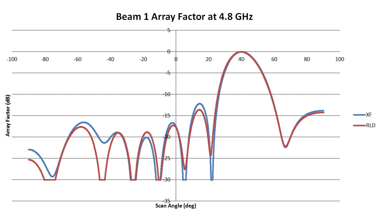
Figure 4: This is a plot of the array pattern for Beam 1 of the 4.8 GHz lens comparing the results from RLD with those from XFdtd. The results are a good match with high correlation between the two plots. The plots for the 9.6, 19.2, and 38.4 GHz lenses are very similar.
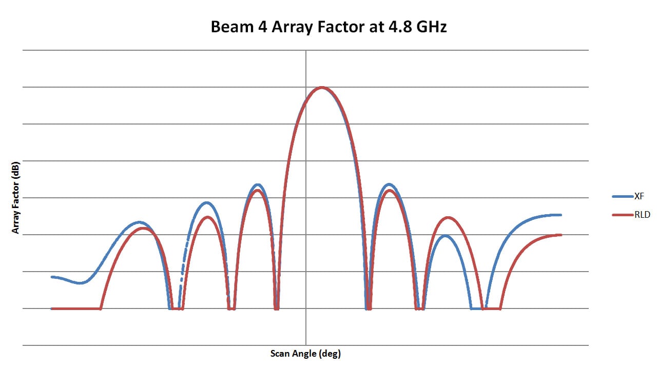
Figure 5: This is a plot of the array pattern for Beam 4 of the 4.8 GHz lens comparing the results from RLD with those from XFdtd. A good match is found with only some slight variation in the side lobe levels. The plots for the 9.6, 19.2, and 38.4 GHz lenses are very similar
The simulations are repeated for 9.6 GHz, 19.2 GHz, and 38.4 GHz with lenses that look very similar to the 4.8 GHz case shown in Figure 3, but scaled accordingly due to the change in frequency. For each case, the substrate thickness drops to maintain well-sized transmission lines. For 9.6 GHz, the substrate thickness is 0.508 mm while at 19.2 GHz and 38.4 GHz it is set at 0.254 mm and 0.127 mm respectively. The resulting beam patterns are also very similar to those shown in Figures 4 and 5 for the 4.8 GHz case.
At 57.6 GHz the design changes slightly because the dielectric substrate selected for use in the lens does not come in thicknesses smaller than 0.127 mm. Because of the thickness of the substrate the transmission lines also become thicker which requires some changes to the layout of the lines. The resulting lens is shown in Figure 6 where the general configuration is a good match to the 4.8 GHz case shown in Figure 3, but clearly the transmission lines are thicker. The resulting beam patterns have high correlation between RLD and XFdtd results as was found in the previous cases. The pattern for Beam 1 is shown in Figure 7 and that for Beam 4 in Figure 8.
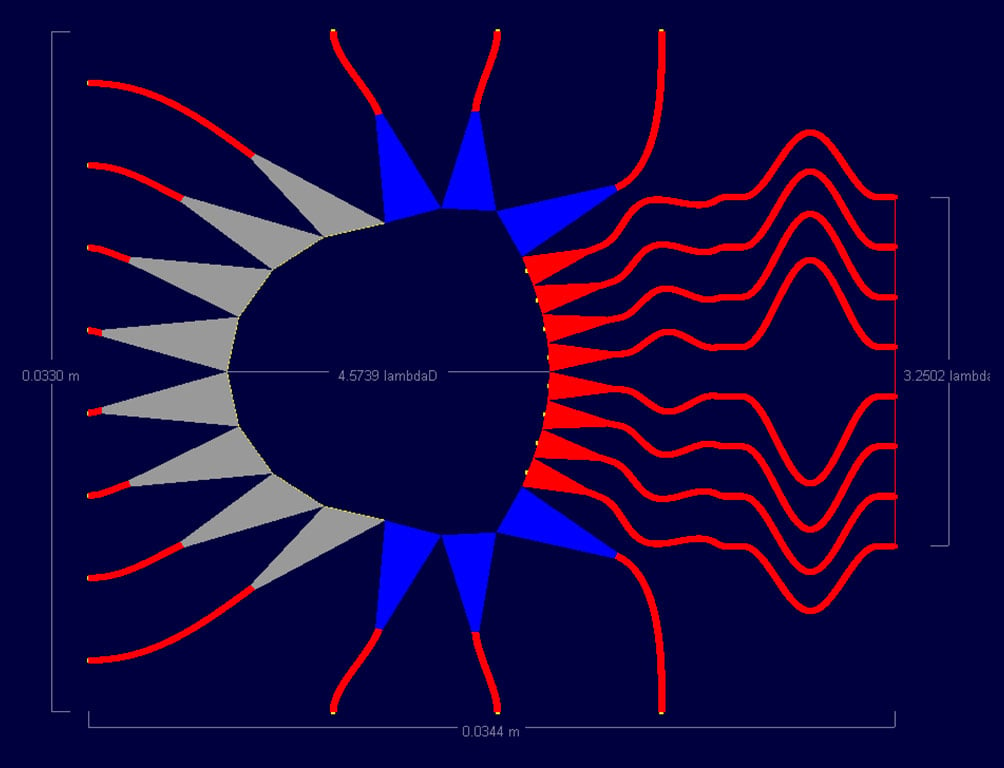
Figure 6: Shown is the lens designed in RLD for the 57.6 GHz frequency case. Here the dielectric constant of the substrate is 3.0 and the thickness is 0.127 mm which is the thinnest sheet for this particular dielectric material. Due to the higher frequency the transmission lines are thicker to maintain 50 ohm impedance for this thickness dielectric. This increases the difficulty of laying out the lines.
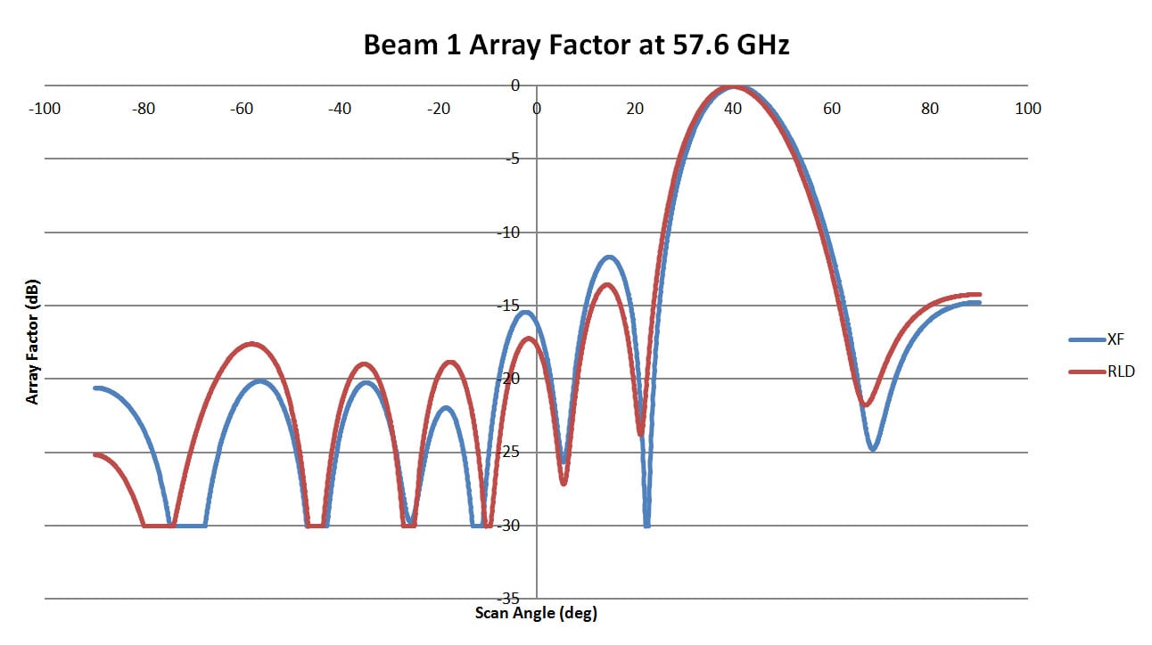
Figure 7: This is a plot of the array pattern for Beam 1 of the 57.6 GHz lens comparing results from RLD with those from XFdtd. The two plots are a good match with high correlation. There is a slight shift in the scan angle of the main beam.
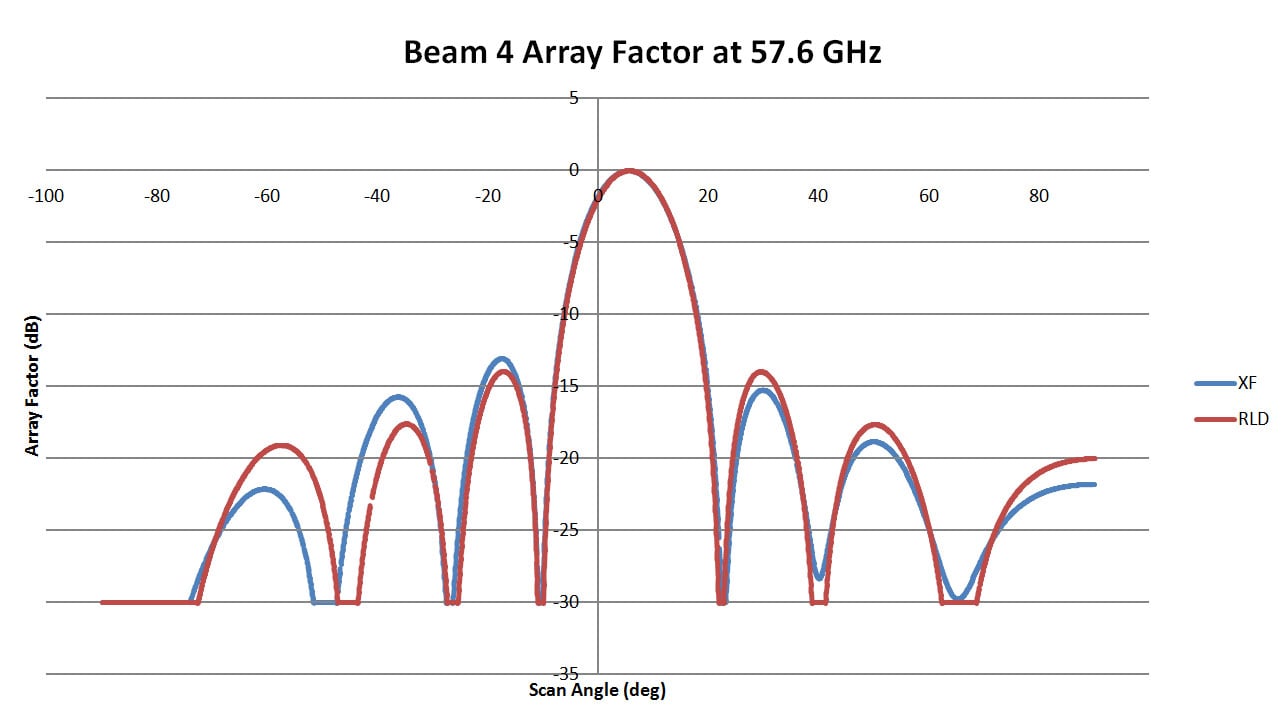
Figure 8: This is a plot of the array pattern for Beam 4 of the 57.6 GHz lens comparing results from RLD with those from XFdtd. The two plots are a good match with high correlation
Finally, the lens is redesigned at 76.8 GHz which is the upper frequency limit for the dielectric material selected for use in the design. Here the design is more challenging due to the thickness of the dielectric material available. The design is repeated three times with different dielectric values to demonstrate the performance for each. Using the substrate with a dielectric value of 3.0 and the minimum thickness of 0.127 mm, the transmission lines become quite thick which makes the subtle bends in the lines difficult to resolve. The lens for the 3.0 case is shown in Figure 9 where the thicker lines are clearly visible. The size of the dummy ports (measured in terms of wavelengths) was also reduced and the number increased to assist in the layout of the lines. When the substrate is changed to the material with a dielectric value of 6.5, the transmission lines become thinner allowing better definition of the curves of the lines as seen in Figure 10. The dummy ports in Figure 10 are larger than those of the 3.0 dielectric case of Figure 9 but still smaller than those used in the lower frequency designs. Finally Figure 11 shows the lens designed with a dielectric value of 11.2 and a 0.127 mm thick substrate. Here the transmission lines are thin and the curvature of the lens sidewalls is reduced slightly to assist in the layout. The resulting beam patterns from the three lenses of Figures 9-11 are relatively consistent as can be seen in Figures 12 and 13. The correlation between results is lower here, primarily due to the variation in the side lobs, but is still over 85% for all cases.
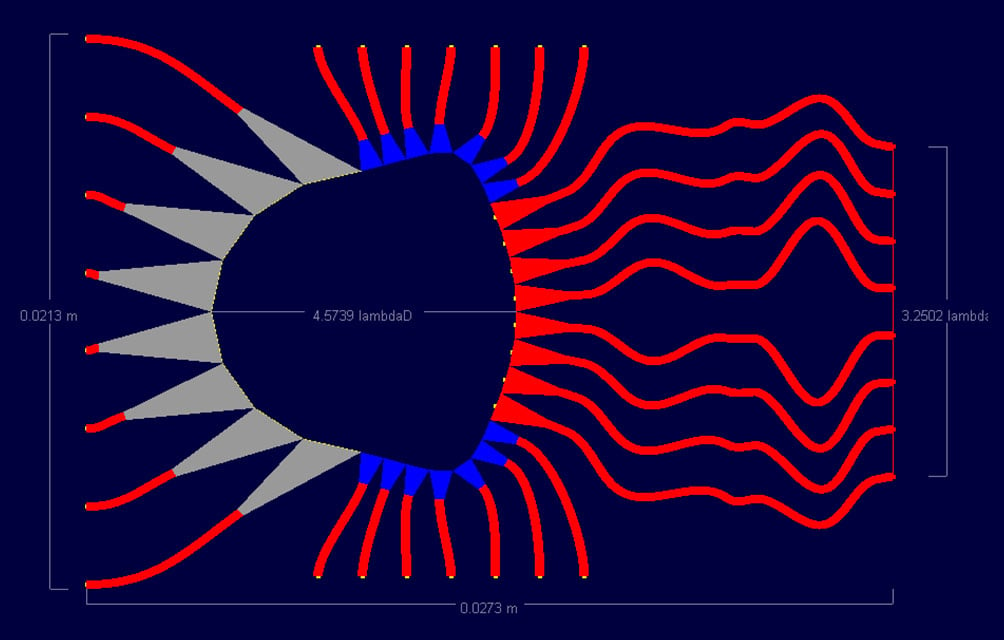
Figure 9: Shown is the lens designed in RLD for the 76.8 GHz lens on a 0.127 mm thick substrate of dielectric constant 3.0. Here the high frequency, thicker substrate size, and lower dielectric constant cause the transmission lines to be quite thick. This makes the line layout difficult resulting in longer array transmission lines to fully resolve the curves and preserve the correct electrical length. The dummy port size is also reduced to aid in the line layout and avoid the dummy lines being too close to the array lines.
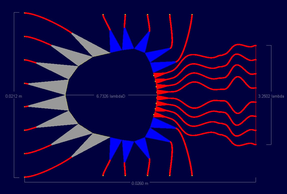
Figure 10: Shown is the lens designed in RLD for the 76.8 GHz lens on a 0.127 mm thick substrate of dielectric constant 6.5. Here the higher dielectric constant makes the transmission lines thinner and aids in the line layout task. The dummy ports are slightly larger than those in Figure 9, but are still smaller than those used for the lower frequency designs.
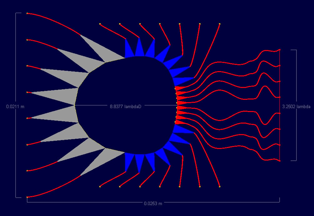
Figure 11: Shown is the lens designed in RLD for the 76.8 GHz lens on a 0.127 mm thick substrate of dielectric constant 11.2. The high dielectric constant makes the lines thin, aiding the layout; however, due to the very small aperture of the array ports, the dummy ports take up a larger portion of the lens. In this case the curvature of the sidewall is reduced slightly to help with the line layout and reduce the number of dummy ports.
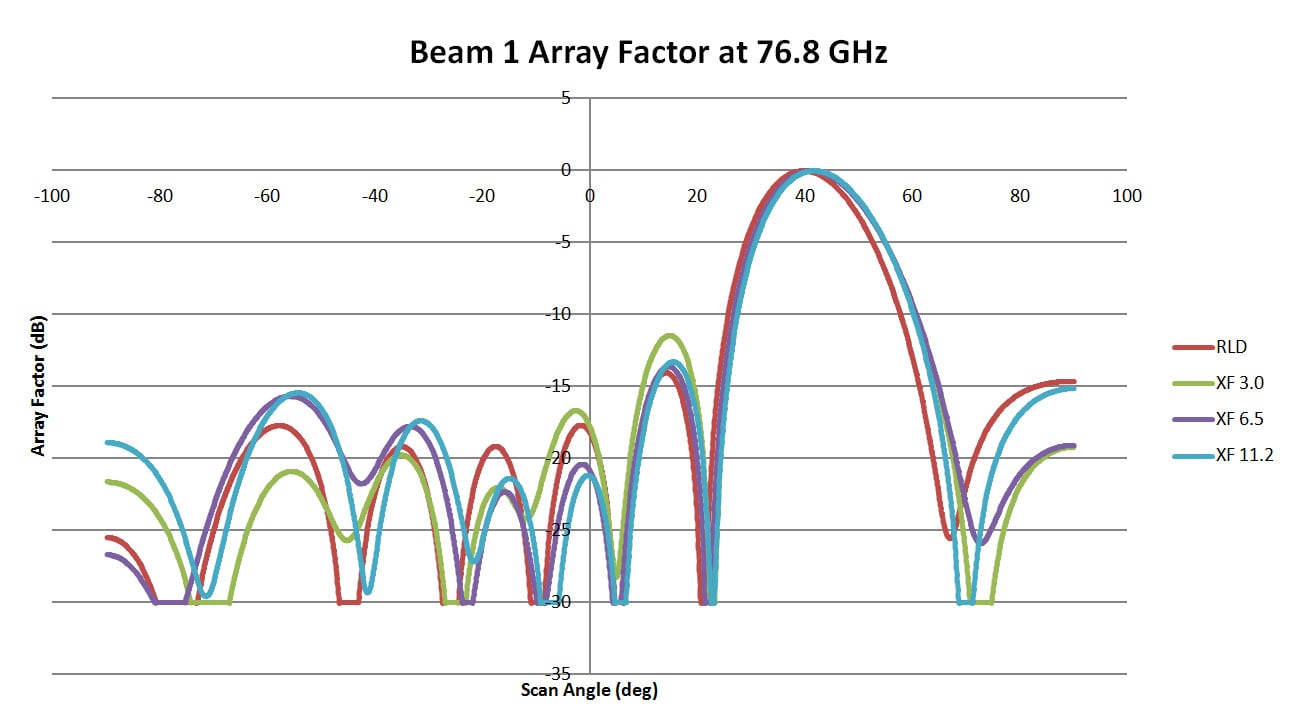
Figure 12: This is a plot of the array pattern for Beam 1 of the three 76.8 GHz lens designs comparing results from RLD and XFdtd. The correlation is slightly lower than in the other cases and there is a more noticeable shift in the main beam angle. However, overall the lens performance is still good.
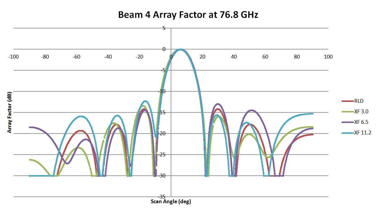
Figure 13: This is a plot of the array pattern for Beam 4 of the three 76.8 GHz lens designs comparing results from RLD and XFdtd. The correlation is slightly lower than in the other cases and from the higher side lobe variation. However, overall the lens performance is still good
Conclusion
This example demonstrates that the RLD software can produce Rotman Lens designs for a wide range of frequencies. In this example the maximum frequency simulated was nearly 77 GHz. The beam patterns produced by the RLD designs were verified by full wave simulations of the XFdtd software and shown to have high levels of correlation indicating that the designs in RLD were valid. It is necessary to mention that the designs made in RLD were carefully considered and it is possible to create a lens in RLD that will give reasonable theoretical results but will fail to produce good results in XFdtd or in actual measurements. Important design considerations are proper selection of substrate dielectric constant and thickness to give well-defined transmission lines and a good layout. In addition, the curvature of the sidewalls in the RLD design is a factor that can have a significant impact on the lens performance. A study of the sidewall curvature is considered in the RLD example Rotman Lens Sidewall Curvature Impact on Performance: RLD vs. XFdtd Simulation Results.
Reference
-
Rotman, W. and R. Turner, "Wide-Angle Microwave Lens for Line Source Applications," IEEE Transactions on Antennas and Propagation, vol. 11, no. 6, pp. 623-632, Nov. 1963.
-
Hansen, R. C., "Design Trades for Rotman Lenses," IEEE Transactions on Antennas and Propagation, vol. 39, no. 4, pp. 464-472, April 1991.