Introduction
This example demonstrates how XFdtd simulates a 60 GHz cylindrical dielectric resonator antenna that is constructed on a silicon base to emulate on-chip designs. The antenna could be used for a wireless personal area network (WPAN), which would provide communication in the immediate vicinity of a user’s workspace. The antenna has a peak gain of about 2.5 dBi, a bandwidth of over 2.5 GHz, and positive gain of about +/- 55 degrees off boresight. The antenna design and simulation discussed here comes from a conference paper [1].
Device Design and Simulation
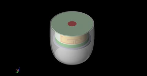
As the antenna is intended to be on-chip, it is simulated here by being attached to a section of a lossy silicon (relative permittivity 11.9, conductivity 10 S/m) block 1500 μm x 1500 μm x 250 μm. A 6.22 μm layer of SiO2 (relative permittivity 4) covers the top of the silicon block and is then covered by a 2 μm layer of conducting ground plane. A 50-ohm co-planar waveguide (CPW) feeds the resonator, which has a radius of 0.33 mm, a height of 0.3 mm, and a high relative permittivity of 48. Vias are installed between the ground plane and the silicon block around the CPW slots. The antenna geometry is visible in a three-dimensional CAD view in Figure 1 and a top-down view in Figure 2.
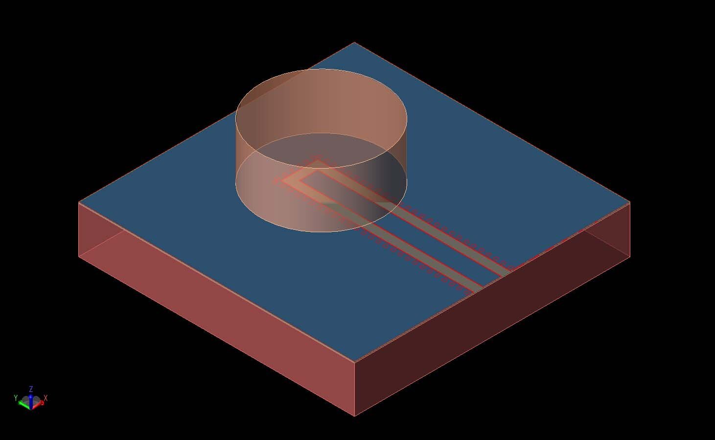
Figure 1: A three-dimensional view of the on-chip dielectric resonator antenna is visible as a CAD drawing. The cylindrical resonator is shown above the co-planar waveguide feed. The silicon base layer is at the bottom.
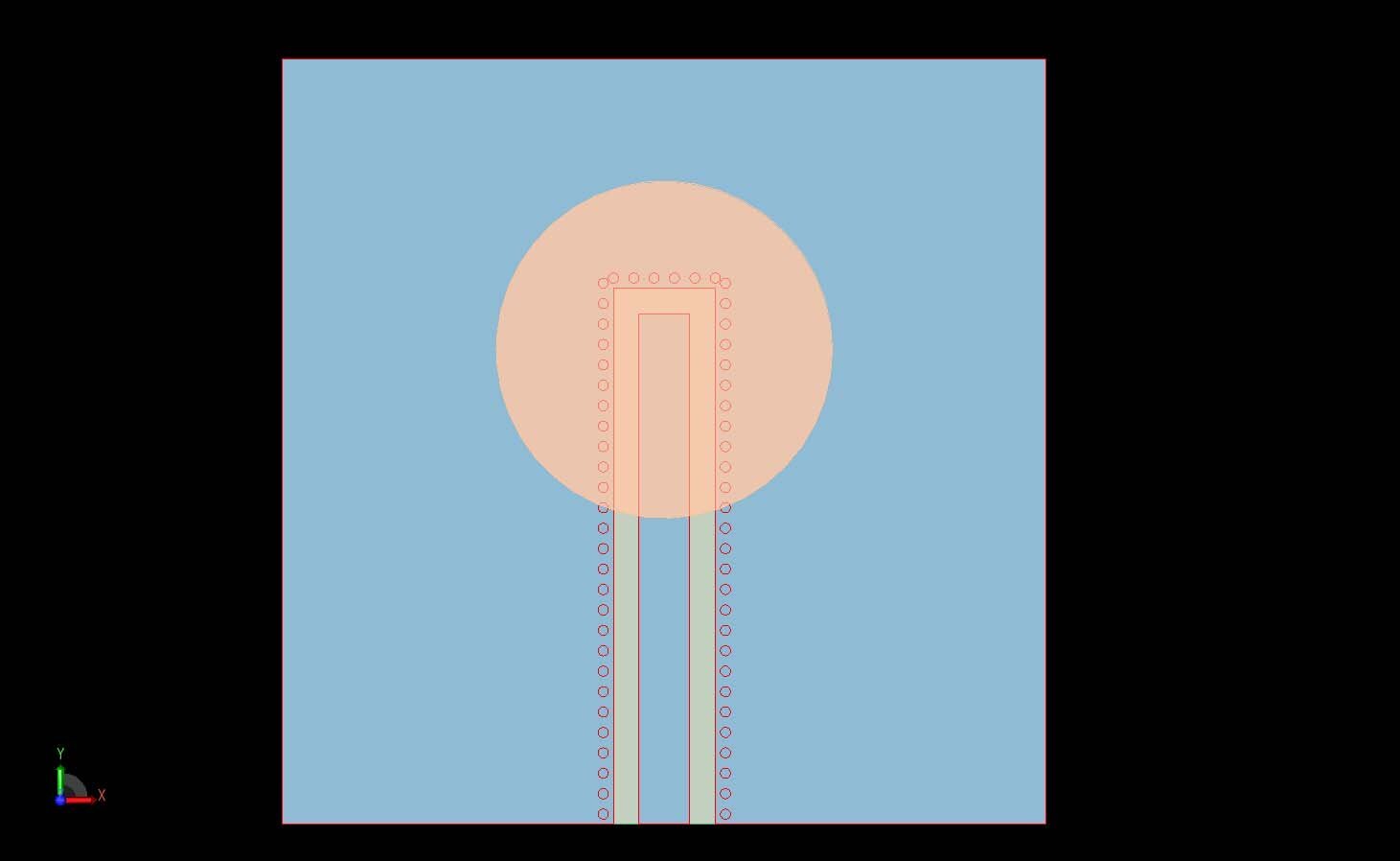
Figure 2: A top view of the antenna is shown where the co-planar waveguide lines are visible as well as the surrounding vias, which ground the conducting layer to the silicon block.
Following simulation, the return loss is found to have a deep null near 60 GHz (Figure 3) with a -10dB bandwidth of more than 2.5 GHz. The input impedance as a function of frequency is plotted in Figure 4, which shows a good match to 50 ohms at 60 GHz.
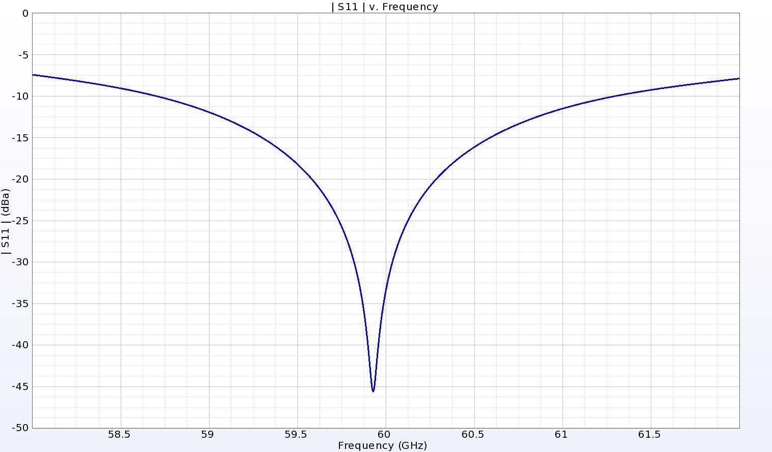
Figure 3: The antenna shows a deep null in the return loss near 60 GHz while still maintaining a -10 dB bandwidth of over 2.5 GHz.
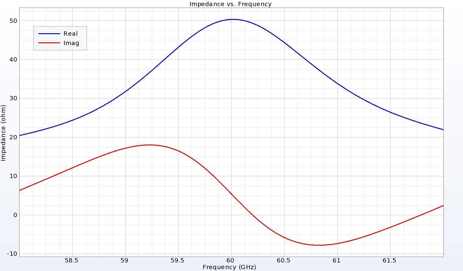
Figure 4: The input impedance of the antenna is well matched to 50 ohms at 60 GHz with smooth transitions through the 4 GHz plot range.
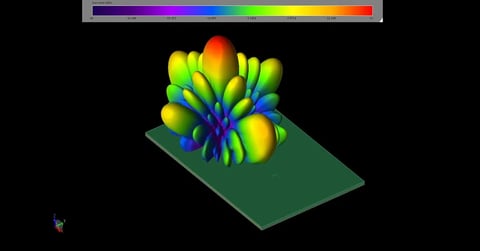
The gain of the antenna as a function of frequency at a point directly above the antenna (Figure 5) shows a peak gain of about 2.5 dBi at 60 GHz, which rolls off smoothly with positive gain at more than 4 GHz bandwidth. The radiation and system efficiencies of the antenna (with and without mismatch losses) show a peak of about 60% at 60 GHz (Figure 6) and the radiation pattern is nearly spherical with positive gain over a range of about 110 degrees (Figure 7). In the YZ and XZ planes (vertical cuts), the antenna has nearly uniform co-polarized gain (Figures 8 and 9) and much lower cross-polarized gain. The radiation pattern in the horizontal XY plane is shown in Figure 10.
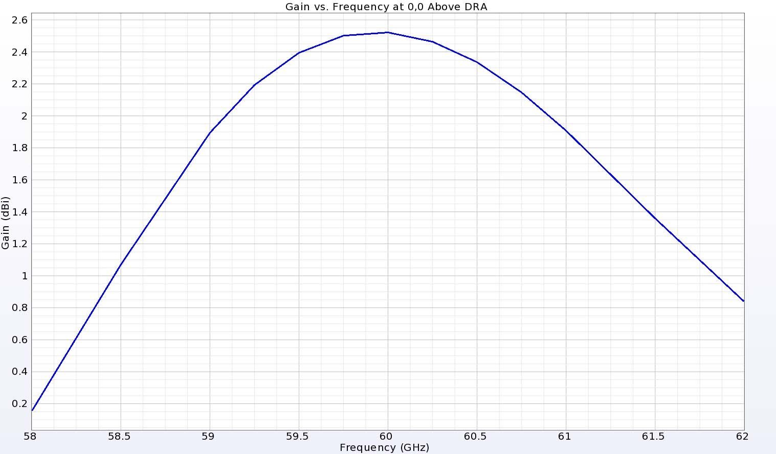
Figure 5: The gain at a point directly above the antenna is shown to peak at about 2.5 dBi at 60 GHz and tapers off smoothly with positive gain over the entire 4 GHz range.
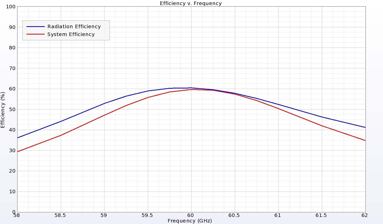
Figure 6: The radiation and system efficiencies of the antenna are quite good at around 60% at 60 GHz due to the reduced losses compared to metal antennas.
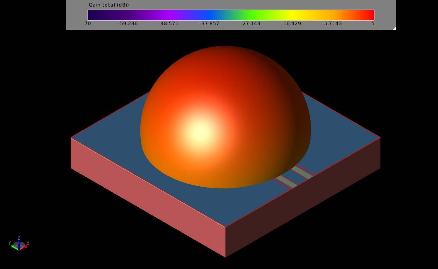
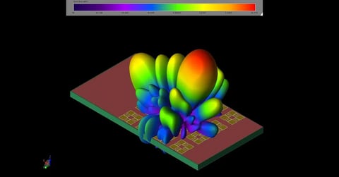
Figure 7: The three-dimensional radiation pattern at 60 GHz shows a nearly spherical distribution. The antenna has positive gain over a 110-degree beamwidth.
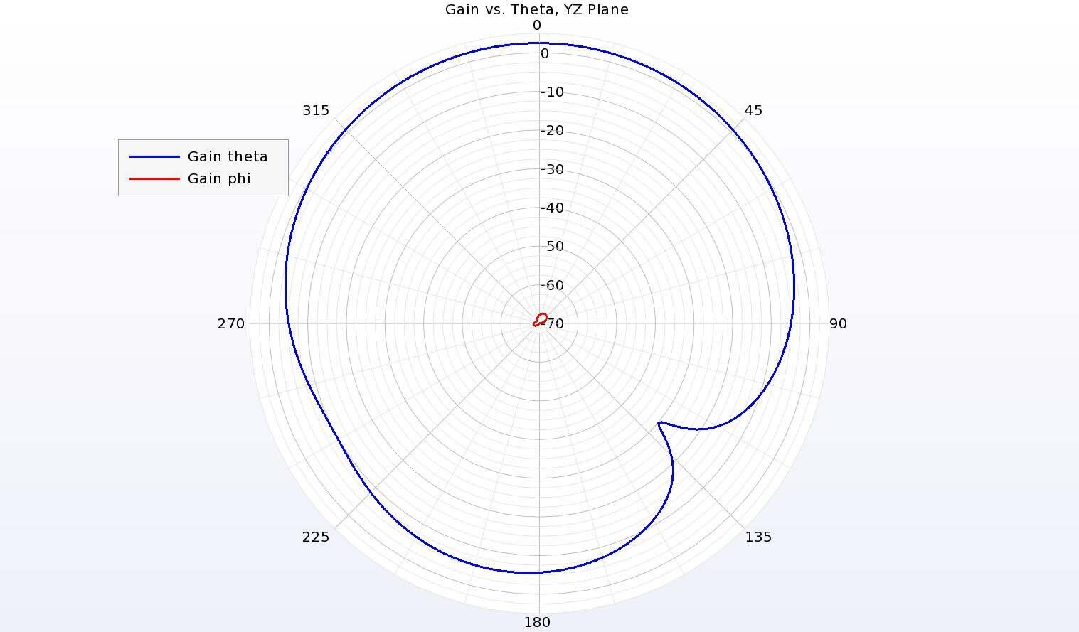
Figure 8: In the YZ plane (vertical cut) of the antenna pattern, the co-polarized gain is seen to be much greater than the cross-polarized gain, offering excellent isolation.
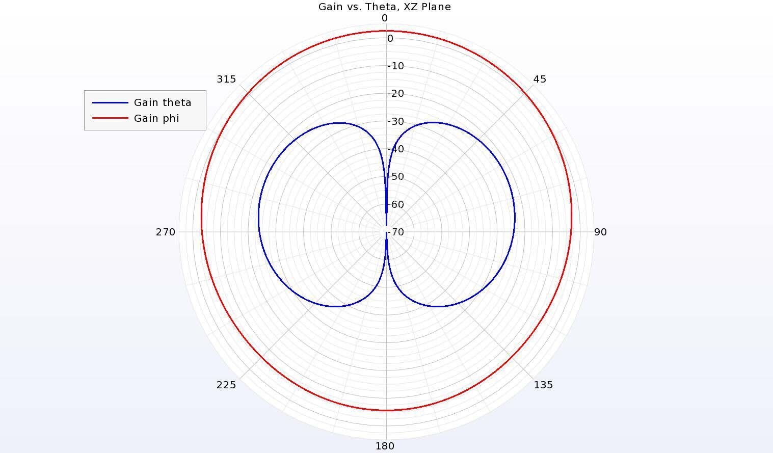
Figure 9: In the XZ plane (vertical cut) of the antenna pattern, the co-polarized gain is nearly 30 dB higher than the cross-polarized gain, providing excellent isolation.
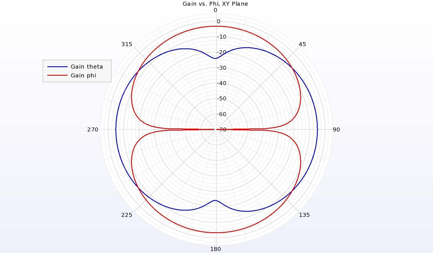
Figure 10: The gain pattern in the horizontal XY plane is reduced with peak gain at -3 dBi and shows a mix of the polarizations.
Conclusion
The high permittivity dielectric resonator of the antenna is able to operate with much lower losses than a metallic antenna, resulting in higher efficiency while still providing good broadband performance for gain and impedance.
Reference:
[1] P. V. Bijumon, A. P. Freundorfer, M. Sayer and Y. M. M. Antar, "On-Chip Silicon Integrated Cylindrical Dielectric Resonator Antenna for Millimeter Wave Applications," 2007 International Symposium on Signals, Systems and Electronics, Montreal, QC, 2007, pp. 489-492, doi: 10.1109/ISSSE.2007.4294520.