.webp "image-asset (3)")


Additional Information
-
Webinars
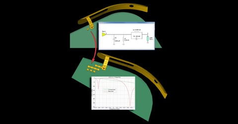
Antenna Design Workflow Using Full-Wave Matching Circuit Optimization
The design of a matched antenna is a fairly involved process. This webinar shows how XFdtd simplifies this process by providing tools to parameterize the unmatched antenna, determine S11, synthesize a matching network topology with Optenni Lab, and determine the final component values using the Circuit Element Optimizer.
Explore Resource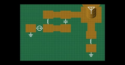
Webinars
Introduction to XFdtd’s Circuit Element Optimizer
Remcom’s Circuit Element Optimizer for XFdtd is a unique tool for full wave matching circuit optimization. This webinar introduces the capability and provides an example of how it is used. A GPS/Bluetooth antenna and an LTE antenna are used for the demonstration.
Explore Resource -

Application Examples
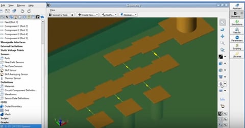
FDTD Simulation: Optimizing an LTE Antenna's Matching Network
A simple antenna for LTE band operation is added to the PC board of a smartphone in XFdtd and the matching circuit is tuned for operation in multiple frequency bands. The component values in the matching network are chosen to maximize system efficiency.
Explore Resource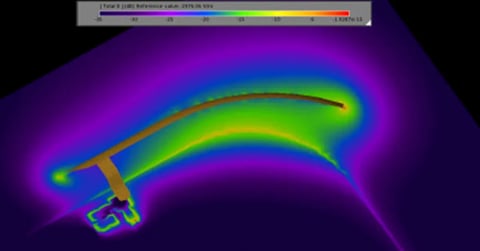
Application Examples
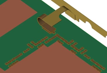
Full Wave Simulation: Matching Network Design for GPS / Bluetooth Antenna
XFdtd's Circuit Element Optimizer is used to determine optimal matching component values for a dual purpose antenna.
Explore Resource -
Videos
Demonstration of Full-Wave Matching Circuit Optimization in XFdtd
This video gives a demonstration of Full-Wave Antenna Matching Circuit Optimization using XFdtd's Circuit Element Optimizer (CEO). The antenna matching circuit design flow is discussed, including C
Explore Resource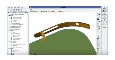
Videos
XFdtd and Optenni Lab Integration for Matching Circuit Design
Remcom's XFdtd 3D EM simulator integrates with Optenni Lab for antenna matching circuit optimization. This brief video shows the highlights of the workflow and integration using a GPS and Bluetooth
Explore Resource -

Publications
Full Wave Matching Circuit Optimization Shortens Design Iterations
Full wave matching circuit optimization (FW-MCO) is a new technology that combines full wave, 3D EM simulation with circuit optimization into a novel approach for solving an age-old RF problem: determining which component values provide the desired match for a given matching network layout. This article describes the design process using the design of a matching circuit for a GPS-Bluetooth antenna.
Explore Resource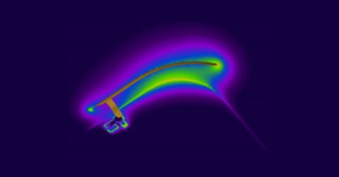
Publications
Overview of XFdtd's Circuit Element Optimizer
XF’s Circuit Element Optimizer utilizes full wave analysis to select the component values for a given printed circuit board (PCB) layout. The tool allows design engineers to optimize matching circuit lumped element values directly in the EM layout where the coupling from multiple antennas and the ground return current paths are taken into account. This whitepaper gives an overview of how the Circuit Element Optimizer works and the benefits it provides.
Explore Resource -
Brochures
Full Wave Matching Circuit Optimization Brochure
Determining the final set of component values in a matching network can be a challenging process. At higher frequencies, especially VHF and above, significant EM effects on the real circuit (inter-connection transmission line effects and coupling between the antenna being tuned, other antennas, and other parts of the structure) are difficult to quantify and account for in circuit schematic simulators alone.
Explore Resource
Save time and reduce costs.
Contact Remcom today for a customized solution to your most complex electromagnetic challenges.
Request a Quote