Introduction
An RFID tag system is examined using XFdtd EM Simulation Software to validate its performance for use in situations where high volume usage requires very low-cost components. This example is derived from a system described in a published journal paper [1]. The RFID tag is constructed as a microstrip device with spiral resonators tuned to specific frequencies that represent separate bits of the tag code. The resonators are connected to two cross-polarized ultrawide band (UWB) monopole disk antennas which receive and transmit the signal from the scanning system. The system is demonstrated with a design capable of encoding six bits that are formed by resonances 100 MHz apart between 2.0 and 2.5 GHz. The testing is done using two cross-polarized log period dipole array (LPDA) antennas which transmit and receive the signal from the RFID tag.
Device Design and Simulation
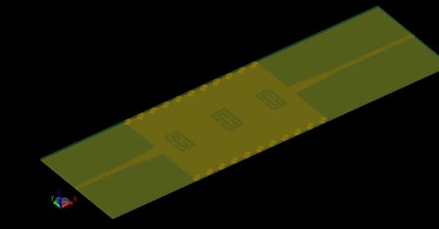
The six-bit RFID tag design is shown in XFdtd in Figure 1, where the red material represents a 0.787 mm thick Taconic TLX0 substrate (relative permittivity 2.45, loss tangent 0.0019) and the green material is perfect conductor material. The two cross-polarized UWB monopole disk antennas are visible at the left (horizontal) and right (vertical) of the center section holding six spiral resonators that form the six bits of the tag. In Figure 2, a close-up view of one of the spiral resonators is shown. The dimensions of each spiral are modified slightly to shift the resonance by 100 MHz for each successive spiral. A ground plane covers part of the back side of the RFID tag under the spiral resonators but not the disk antennas.
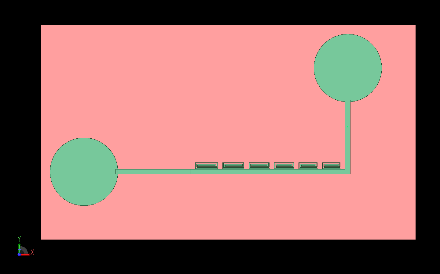
Figure 1: The RFID tag consisting of two UWB monopole disk antennas and six spiral resonators is shown as a CAD model in XFdtd.

Figure 2: A detailed view of one of the spiral resonators is shown. The dimensions of the spiral are changed slightly to shift the resonance of the spiral and create a different bit for the RFID tag.
The system receives a signal from an external source that is polarized with one of the two antennas. The resonances from the spirals are then transmitted via the second, cross-polarized, antenna and received by a second external antenna in the matching polarization. The antennas are cross-polarized to reduce the amount of cross-talk between them and isolate the signal from the RFID tag.
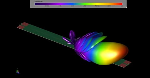
The UWB monopole disk antenna shown in Figure 3 is analyzed alone initially. It is found to have a typical monopole pattern with even gain for the co-polarized case in the azimuthal direction (Figure 4) and low cross-polarized gain (Figure 5). The return loss for the antenna is at acceptable levels for a very broad frequency range, as shown in Figure 6.

Figure 3: The UWB monopole disk antenna is shown as a CAD model in XFdtd.
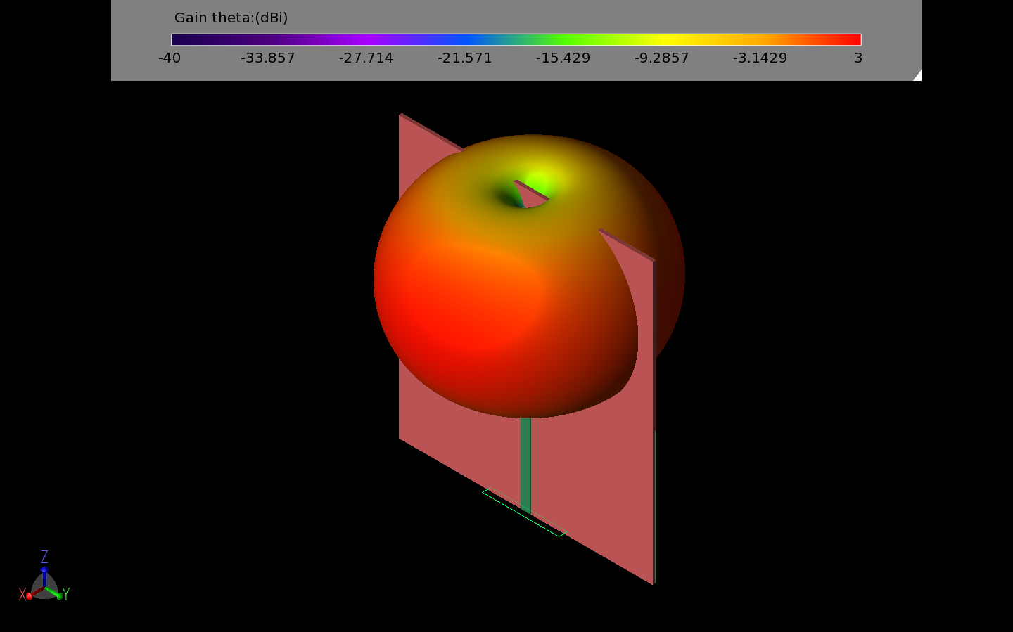
Figure 4: The co-polarized gain pattern of the UWB monopole disk is uniform around the antenna.
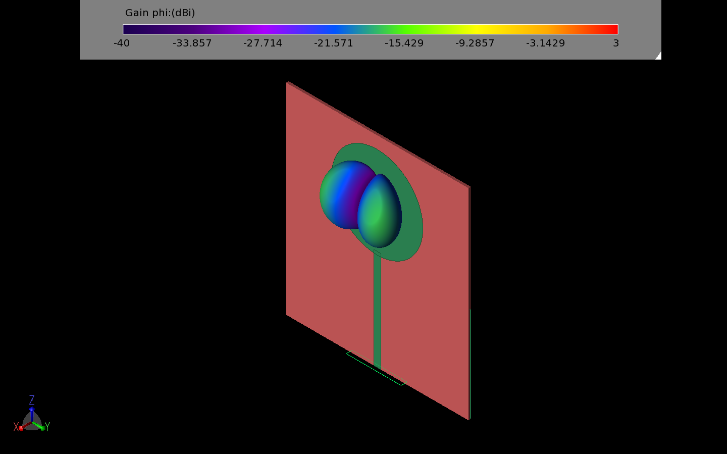
Figure 5: The cross-polarized gain pattern of the UWB monopole disk antenna has very low gain which aids to reduce any cross-talk interference in the RFID tag.
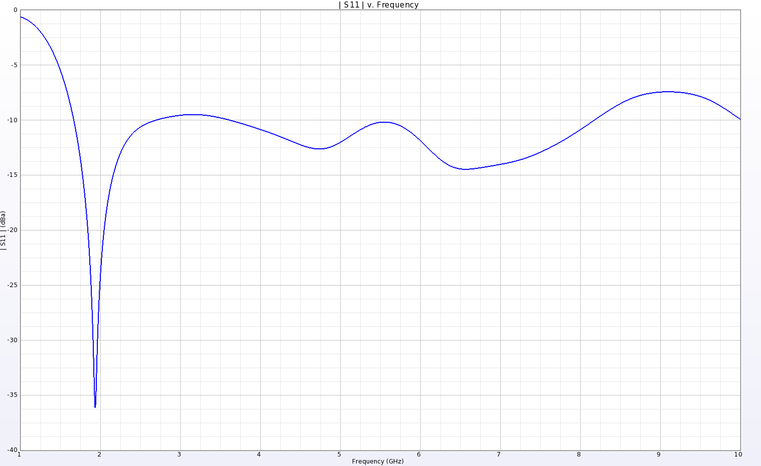
Figure 6: The return loss of the UWB monopole disk antenna shows good performance over a broad frequency range.
The dimensions of the spiral resonators, shown in Figure 7, at the center of the RFID tag are tuned so that each one represents a single bit from 2.0 GHz to 2.5 GHz in even 100 MHz intervals. When simulated alone, the resonators are shown to produce deep nulls at the desired frequencies in the S21 magnitude plots as shown in Figure 8. The phase of the S21 signal may also be used to signify a bit by detecting the phase shifts at certain frequencies. This is demonstrated in Figure 9 where a steep phase shift is located at each of the desired locations between 2.0 and 2.5 GHz.

Figure 7: A six element RFID tag is shown which will produce a six-bit code for the RFID tag.
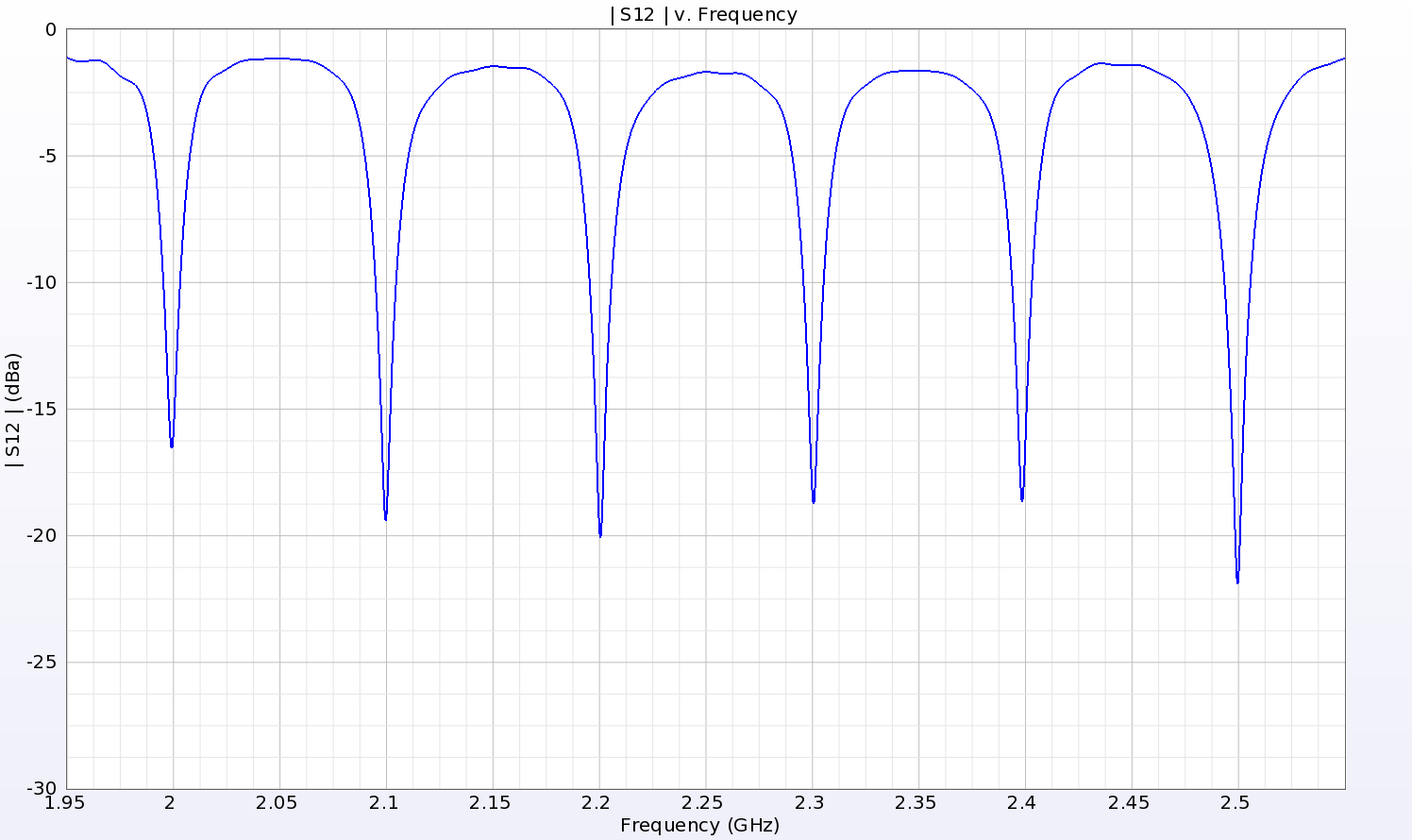
Figure 8: The amplitude response of the RFID tag when analyzed by itself shows clear definition of the six bits from 2.0 to 2.5 GHz. Here the response of 000000 is shown.
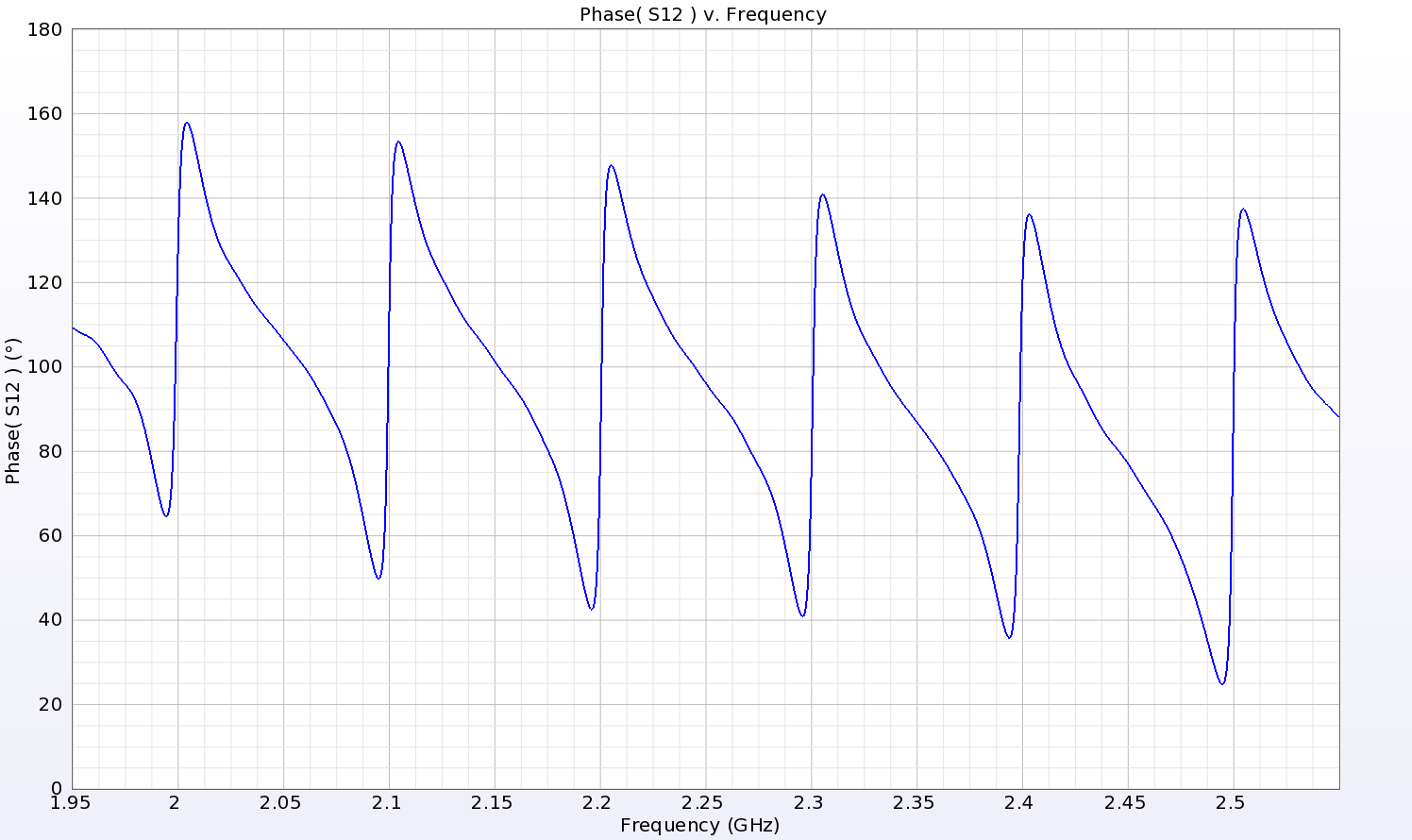
Figure 9: The phase response of the RFID tag when analyzed by itself shows steep phase shifts at each of the six bit locations for the 000000 tag.
To test the performance of a full system, an external source is needed to send a signal to the RFID tag and receive the coded response from it. This is handled by two cross-polarized LPDA antennas. One of the LPDA antennas is shown in Figure 10. The LPDA is designed to transmit a strong co-polarized signal in the forward direction with low cross-polarized gain. The co-polarized gain of the LPDA at 2.0 GHz is shown in Figure 11. The gain in the forward direction (peak gain location) is plotted versus frequency in Figure 12. The initial design of the LPDA has less than desirable return loss performance, so a matching circuit is added to the input port. The matching circuit consists of a series inductor and a parallel capacitor added to the voltage source feed. The result is much improved return loss over the frequency range of interest, as shown in Figure 13.
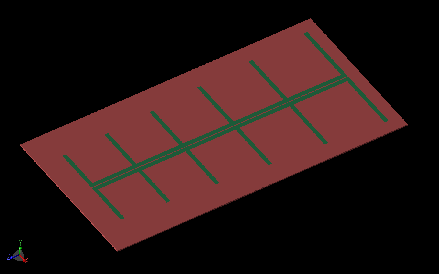
Figure 10: One of the LPDA antenna models is shown in XFdtd.
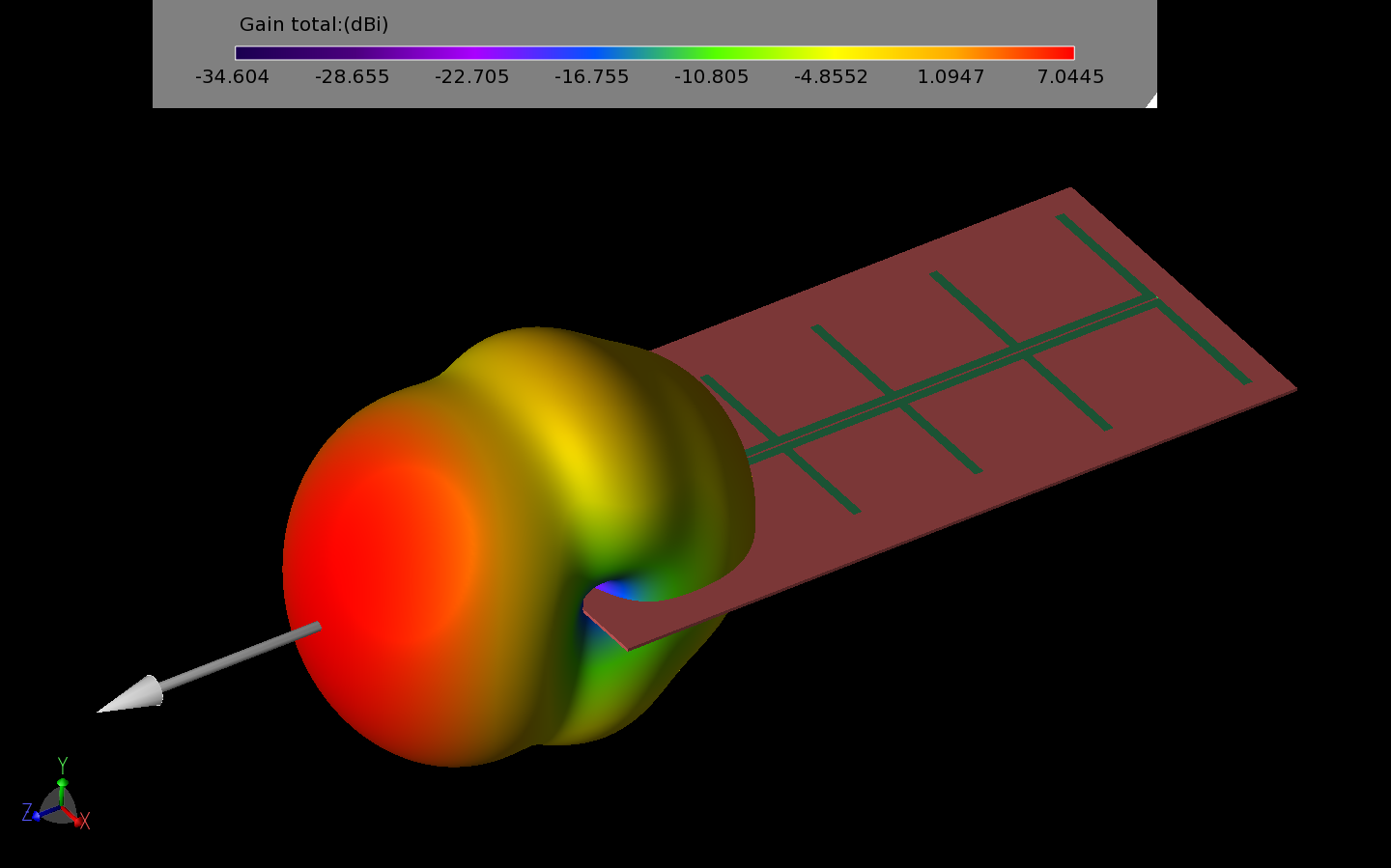
Figure 11: The pattern of the LPDA antenna has strong forward gain and low cross polarization.
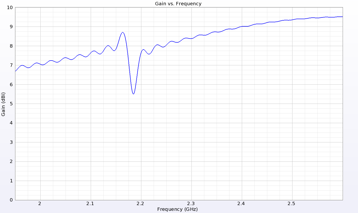
Figure 12: The forward gain of the LPDA antenna is above 7dBi over a broad frequency range.
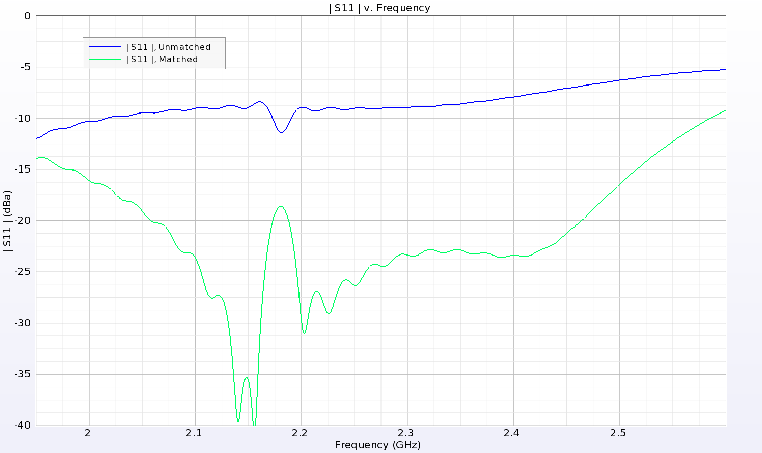
Figure 13: The return loss of the LPDA antenna is greatly improved by the addition of a simple matching circuit and shows very good performance over the entire range of interest.
To test the entire system, two LPDA antennas are placed 5 cm away from the RFID tag with one of the LPDA antennas aligned with the vertical monopole and one aligned with the horizontal. The RFID tag is tested for three different bit combinations of 000000 (all spirals resonating), 010101, and 111111 (all spirals shorted). The shorting of a single spiral and thus the setting of a bit to 1 is performed by adding a small square of conductor onto the spiral as shown in Figure 15. The output of the combined system is displayed using the results of the 111111 tag as a reference as was done in the original paper. This improves the visibility of the tag nulls as it removes the responses introduced by the testing system. The adjusted amplitude plot for the 000000 tag is shown in Figure 16 and the nulls representing the six bits can be clearly seen as having several dB of difference. The adjusted amplitude plot for the 010101 tag is shown in Figure 17 and again the three bits at 2.0, 2.2, and 2.4 GHz are represented by nulls at those locations. Similarly, the phase response is normalized with the 111111 tag signal, and the 000000 tag phase is shown in Figure 18 while that of the 010101 tag is in Figure 19; in each case the phase shifts at the bit locations are visible.
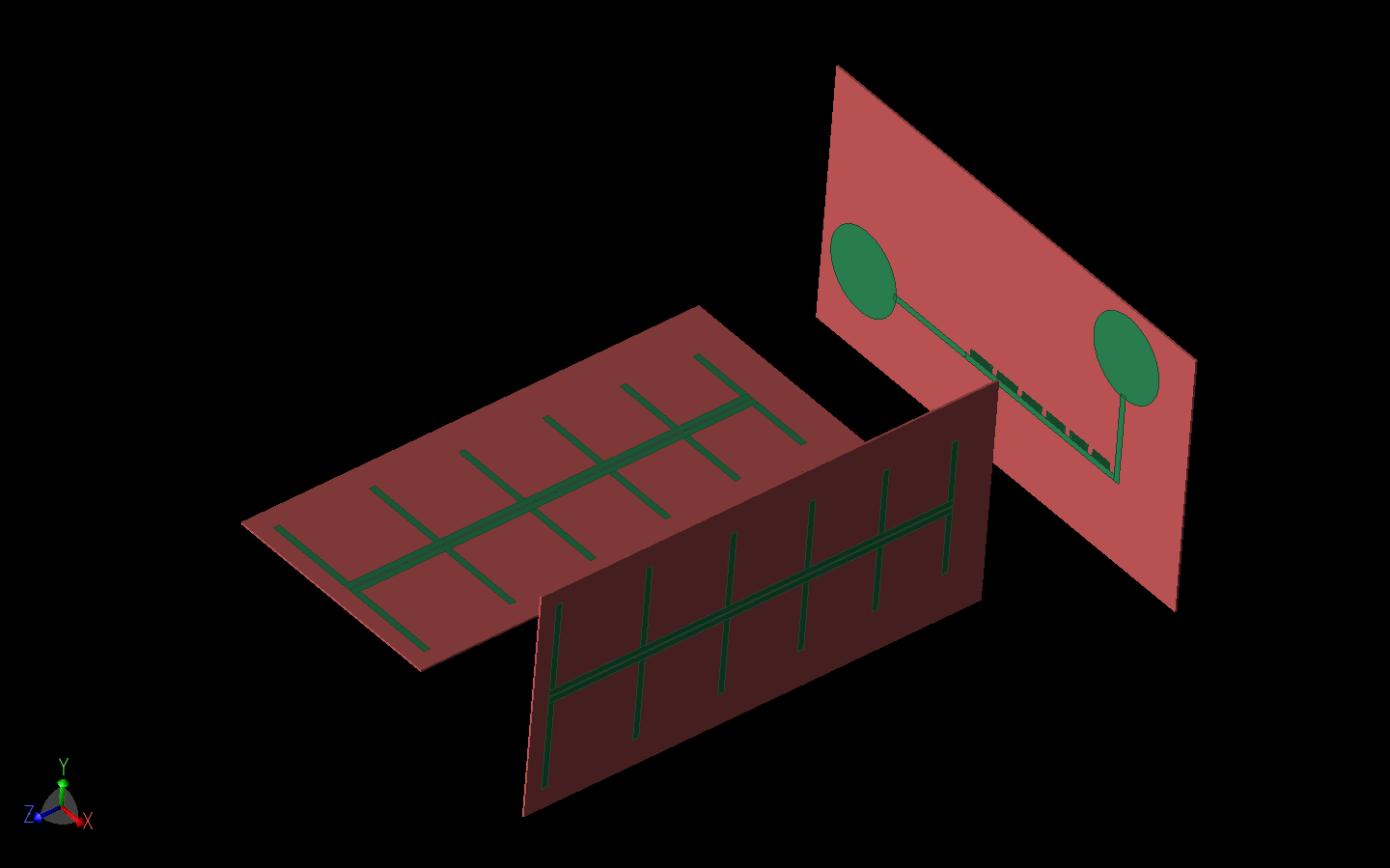
Figure 14: The full RFID system is shown with cross-polarized LPDA antennas for transmit and receive and the RFID tag with cross-polarized UWB disk antennas and the six spiral resonators. The tag is 5 cm away from the transmit/receive antennas.

Figure 15: The bits are set from 0 to 1 by the addition of a short across the spiral arms. This removes the resonance of the spiral from the frequency range of interest.
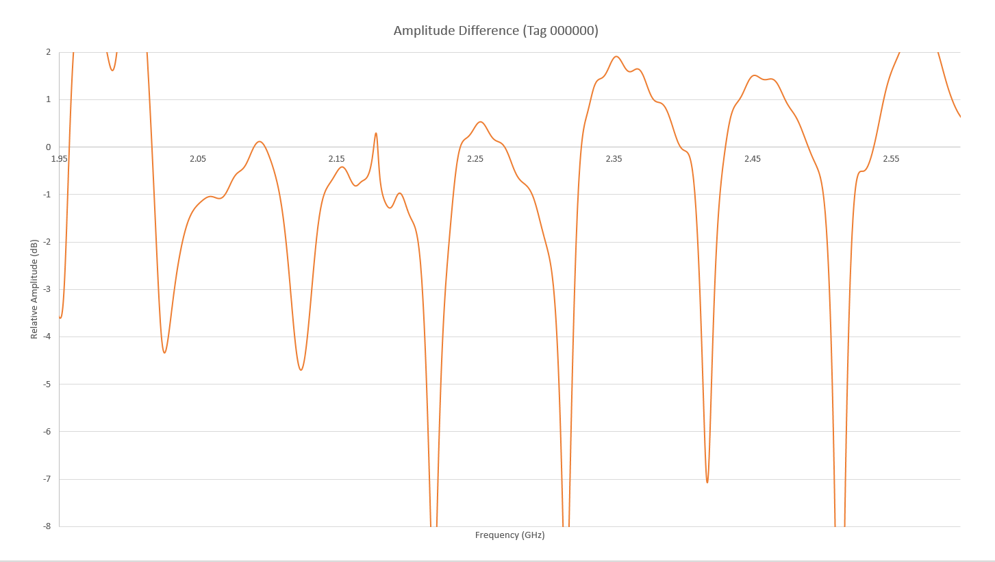
Figure 16: The adjusted amplitude response of the RFID system is shown for the 000000 tag. Here the response of the tag is shown as after normalizing with the response of the 111111 tag for clarity.
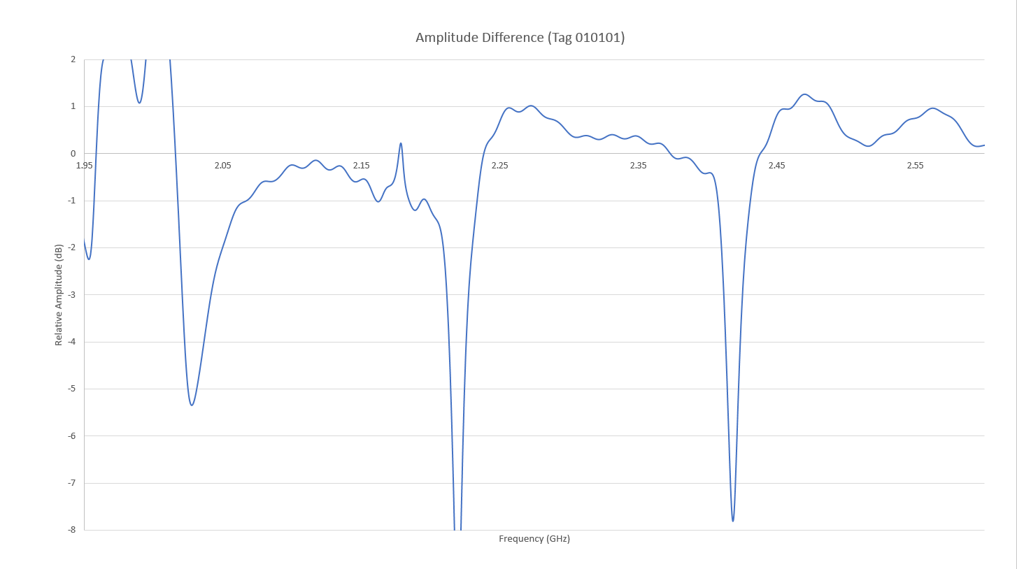
Figure 17: The adjusted amplitude response of the RFID system is shown for the 010101 tag where the three 0 bits are visible at 2.0, 2.2, and 2.4 GHz.
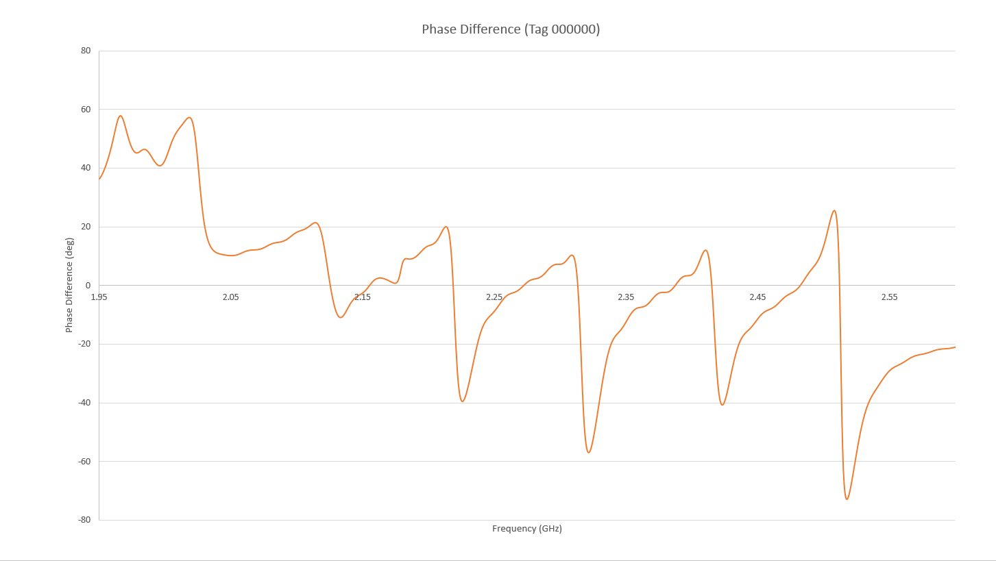
Figure 18: The adjusted phase response of the RFID system is shown for the 000000 tag where the 0 bits are visible as steep phase shifts 100 MHz apart from 2.0 to 2.5 GHz.
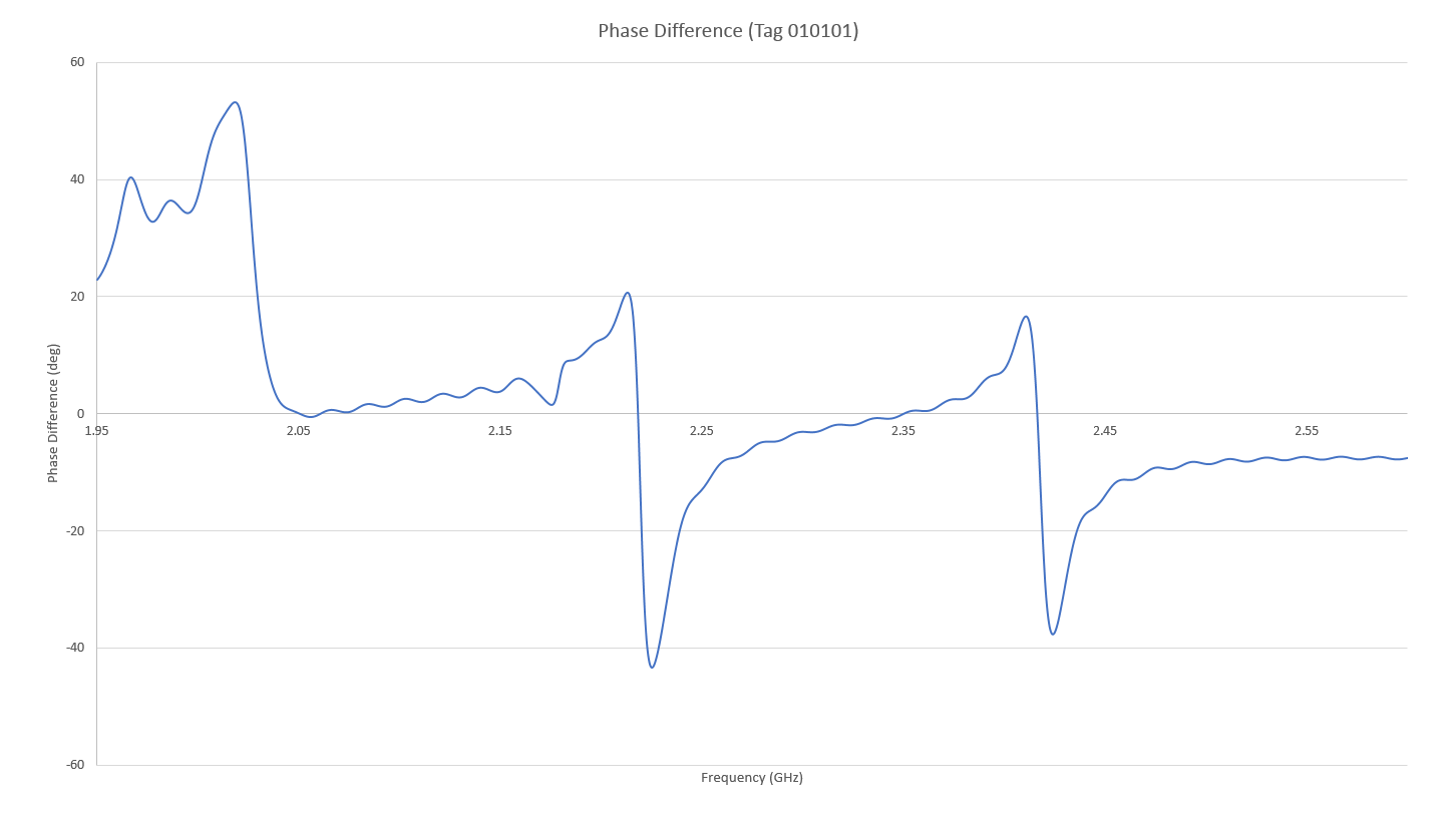
Figure 19: The adjusted phase response of the RFID system is shown for the 010101 tag where the 0 bits are visible as steep phase shifts at 2.0, 2.2, and 2.4 GHz.
Summary
This example has demonstrated the performance of a low-cost, chipless RFID tag system that uses spiral resonators to denote the bits. The performance of the resonators is shown to be quite good when tested alone with very clear indications of the bit signal present in the S-parameter data. When combined into a full system with transmit and reader antennas separated by several centimeters, the system produces recognizable bit patterns, proving the design is feasible.
Reference:
[1] S. Preradovic, I. Balbin, N. C. Karmakar, and G. F. Swiegers, “Multiresonator-Based Chipless RFID System for Low-Cost Item Tracking,” IEEE Trans. Microwave Theory and Techniques, vol. 57, no. 5, pp. 1411-1419, May 2009.