 Several full-wave electromagnetic simulator software products solve Maxwell’s equations in three dimensional detail, using different EM formulations and approaches in order to address high frequency applications such as signal integrity, microwave circuits, and antennas. 3D planar formulations are sometimes referred to as 2.5D or “two and a half D.” Other products are fully arbitrary 3D.
While the capabilities and application areas of planar MoM and fully arbitrary 3D EM simulators overlap extensively in microwave circuit and antenna design, the two different EM simulation categories each have strengths and limitations beyond the basic dimensionality of the tools.
This paper, featured in the July 2015 issue of Microwave Journal, provides a technical comparison of 3D planar EM simulation with fully arbitrary 3D EM simulation and informs users as to which EM approach/formulation may work best for a given application.
Introduction
Several full-wave electromagnetic (EM) simulator software products solve Maxwell’s equations in three dimensional detail, using different EM formulations and approaches in order to address high frequency applications such as signal integrity, microwave circuits, and antennas. 3D planar formulations, such as Sonnet from Sonnet Software, Momentum from Keysight Technologies (formerly Agilent), and Axiem from Applied Wave Research (part of National Instruments), are sometimes referred to as 2.5D or "two and a half D." Other Products such as Remcom’s XFdtd, Ansys’ HFSS, and CST’s Microwave Studio (MWS) are fully arbitrary 3D. Both 3D planar and fully arbitrary 3D EM simulation are full wave, capturing all metal coupling in all three dimensions, but the 3D planar formulations limit what dielectric and metal shapes can be modeled and simulated. The technical comparison of 3D planar EM simulation with fully arbitrary 3D EM simulation helps illustrate by comparison how both formulations work and informs users as to which EM approach/formulation may work best for a given application.
Layered Dielectrics in Planar MoM
Planar MoM formulations are based on parallel, uniformly thick dielectric layers with parallel metal layers in between those dielectric layers. The dielectric layers generally extend horizontally to the end of the simulation space. Fully arbitrary 3D EM simulation allows any dielectric and any metal shapes to be modeled and simulated. The term ͞fully arbitrary 3D comes from the ability of EM simulators like XFdtd, MWS, and HFSS to model and simulate any shape or configuration of metals and dielectrics that one needs. Fully arbitrary 3D EM simulation can simulate three dimensional metal shapes including car body sections, coaxial connector SMA launches, printed circuit board edge connectors, horn antennas, curved wire bonds, and flexed MEMS switches. Planar MoM finds widespread use in electronic design flows because many circuits consist of multiple layers of planar, parallel circuit traces connected vertically by vias. This includes both printed circuit board and integrated circuit technologies.
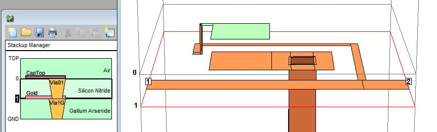
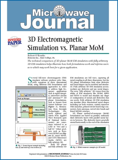
Figure 1: Sonnet layout example including vias on right with cross section of stack up on the left
Figure 2: XFdtd connector example of a 3D model
Mesh Elements and What Gets Meshed
One of the most fundamental differences between planar method-of-moments (MoM) and fully arbitrary 3D EM simulation is meshing: 1) the nature of mesh elements and 2) what parts of the structure get meshed. Meshing, sometimes called subsectioning or gridding, characterizes full-wave EM simulators and distinguishes them from closed-form, equation-based modeling found in circuit simulations. But 3D planar and fully arbitrary 3D EM simulators mesh a design structure very differently from one another. Fully arbitrary 3D EM simulators use a three dimensional mesh element, perhaps a hexahedron (six-sided brick shape) or a tetrahedron (four-sided) shaped mesh element. These three dimensional mesh elements are also referred to as volumetric mesh elements because they occupy a three dimensional volume. By comparison, planar method-of-moments (MoM) simulators such as Sonnet, Momentum, and Axiem, use two dimensional mesh elements. These flat 2D mesh elements can be rectangles or triangles.
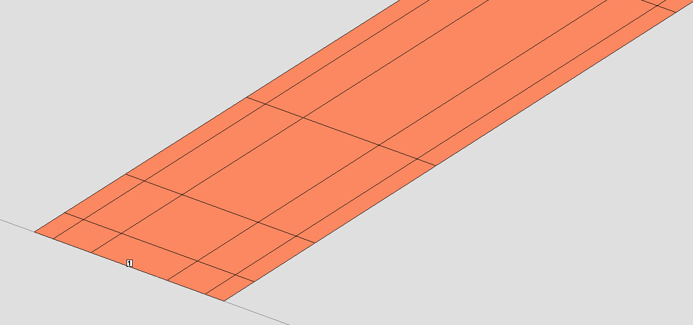
Fig. 3: Sonnet planar 3D MoM stripline subsectioning
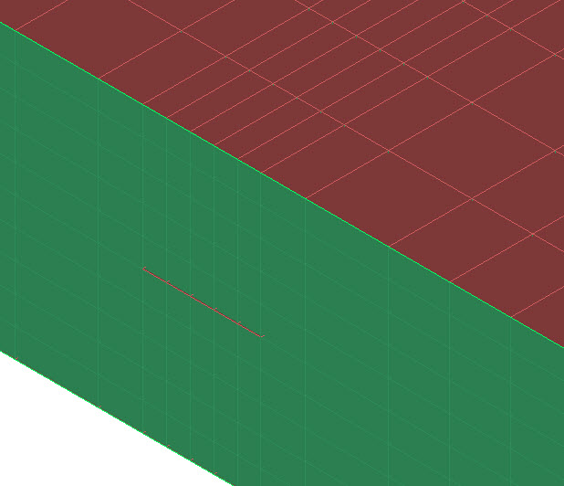
Fig. 4: Remcom XFdtd 3D stripline grid
Next, fully arbitrary 3D simulators also mesh the entire volume of the given simulation problem. Planar MoM simulators mesh only the flat/planar metal conductor surfaces. Taking microstrip transmission lines as an example, fully arbitrary 3D EM simulators mesh the substrate, the metal signal conductor, and the air above the microstrip circuit. By comparison, planar MoM meshes only the flat metal planar conductor (including vertical vias). Planar MoM does not mesh the dielectric substrate nor the air above the microstrip. The effects of the substrate dielectric and the air above the microstrip are taken into account through the Green’s function in planar MoM.
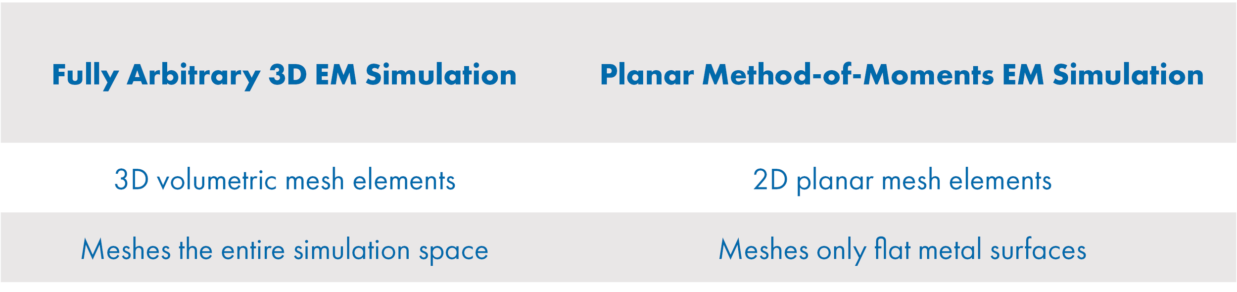
Table 1: Comparison of meshing between planar and fully arbitrary 3D EM simulation
Note that both approaches are full-wave EM simulation; both approaches solve Maxwell’s equations in three dimensions and provide high accuracy results. Both fully arbitrary 3D and planar MoM EM simulations capture all coupling among all metal conductors in all three dimensions of the entire simulation problem space. A two dimensional mesh element in planar MoM simulation in no way implies a two dimensional simulation; planar MoM captures all of the coupling among all of the metal including coupling in the vertical third dimension - hence the name "planar 3D." (By contrast, a two dimensional simulation is more often associated with static solvers for printed circuit board vertical stack up cross sections. These are not discussed in this paper.)
In all EM simulation types, the meshing/gridding/subsectioning is critical to simulation success and demands attention and understanding. The geometric features of the structure being simulated, including both size and spacing, influence the size or density of the mesh; this in turn influences the simulation time or problem size or both. Generally one wants to have three to five mesh elements in the cross section of transmission lines in order to simulate the transmission line impedance and current density (and therefore coupling) accurately. Also, one wants to have at least one mesh cell between two nearby metal conductors in order to differentiate them. Inspecting the mesh before simulation helps ensure these minimum requirements. Automation of meshing in EM simulator software can help reduce the number of required steps one must always take for a given simulation, but do not rely on automatic features to replace the engineer’s judgment. These meshing concepts are very similar among all types of EM simulation.
Vertical Metal and Vias
Planar MoM modeling and simulation is limited in the vertical direction. Planar MoM simulators can simulate horizontal metal with virtually arbitrary shapes in parallel horizontal planes, but planar 3D MoM can only simulate limited configurations of vertically oriented metal, typically based around vias. Fully arbitrary 3D EM simulators can model any shapes of vertical metal including slopes and curves; fully arbitrary 3D EM simulation can simulate currents and fields in all three dimensions anywhere around this metal. Generally planar MoM vertical metal vias carry vertically directed currents. Some planar MoM simulators only simulate uniform currents between adjacent metal layers; some planar MoM simulators simulate variation of vertical current with distance along vias.
Antennas illustrate the distinction between arbitrary vertical metal and planar metal. Patch antennas, where the metal lies on a flat plane, parallel to the dielectrics, work well in planar MoM simulators. A via might feed signal to the metal patch surface from below, perhaps representing a vertically oriented coaxial cable center conductor.
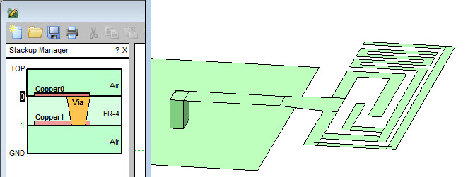
Figure 5: A planar antenna example in Sonnet
A helical or horn antenna clearly needs generalized 3D metal and dielectric modeling capability and requires a fully arbitrary 3D EM simulator. (Please note that there is another class of EM simulation not considered here; some 3D surface MoM or wire-based EM methods work well on antennas.)
Via Fences and Lateral Currents
When spaced closely together in a fence-like manner, planar MoM vias can be used to approximate vertical metal walls, though there may be some limitations on the diagonal flow of currents in those walls. Each via may carry a certain (vertical) current and the amount current varies among the many vias. In fully arbitrary 3D EM simulation, metal can take the form of a via, a metal wall, or any other shape. Fully arbitrary 3D can simulate currents and fields in all directions in and around metal walls. In some sense, vias represent a good distinction between the strength of planar MoM and fully arbitrary 3D. If the circuit consists generally of horizontal metal dominating the circuit behavior and vias taking a minor role, then planar MoM may work well. When one needs to see the details of individual vias, such as exact current densities in three dimensions within one via or a metal wall, then perhaps fully arbitrary 3D may work better for the application. Understanding exactly how an EM simulator models current flow, current variation, and field strengths is important to applying an EM simulator to a structure with vias.
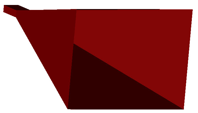
Figure 6: A horn antenna
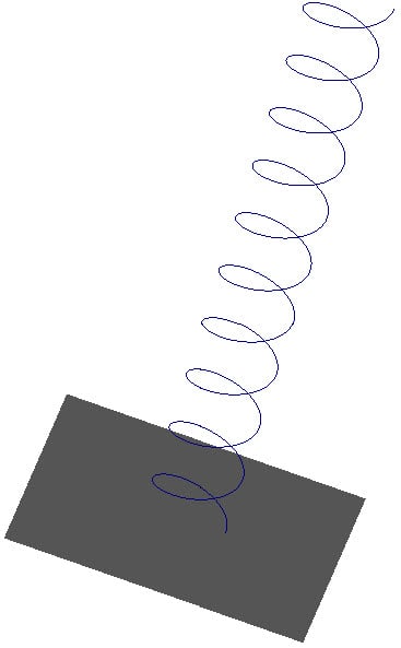
Figure 7: A helical antenna
Simulation Space Boundaries
Planar 3D and fully arbitrary 3D EM simulators all have some kind of simulation space and boundaries surrounding the structure being simulated. Fully arbitrary 3D EM simulation has a six-sided simulation space with a choice of boundary conditions including perfectly electrically conducting (PEC), perfectly magnetically conducting (PMC) and absorbing boundaries. Planar MoM simulation boundaries vary between the two main formulations of MoM. In shielded formulation MoM, such as Sonnet, the simulation space is a six-sided box where the four vertical side walls are always perfectly conducting. The top and bottom of the Sonnet box can be set to PEC, lossy metal material, or 377 ohms simulating open. Unshielded formulations of MoM, such as Axiem from AWR/NI and Momentum from Keysight Technologies, have an infinite ground plane and unbounded open upper and lower hemispheres.
It can be important to match the simulation boundary specification as close as possible to the real boundaries around the physical structure. A PEC boundary on the end of a simulated transmission line dielectric will cause a reflection to signals incident on the boundary. If the physical structure hardware does not have that same PEC or conductive metal boundary, the simulation will mismatch the measurements of the hardware. In the simulation of patch antennas, there can be surface wave energy moving laterally in the substrate above the ground plane and below the patch. A PEC simulation boundary would reflect the surface wave energy back through the substrate.As a comparison experiment, changing lateral simulation boundaries on the patch antenna substrate from open/absorbing to PEC, in a fully arbitrary 3D EM simulator, might give an indication how much difference this surface energy bounding makes to the antenna behavior. In an unshielded formulation of MoM, there is no lateral boundary; surface wave energy goes horizontally away from the patch forever.
It is also possible to use simulation boundaries as part of the structure being simulated. The simulation of stripline, for example, has two ground planes -- one above and one below a stripline center conductor. Instead of putting metal ground conductors explicitly into the simulation model, one could use the PEC boundaries as ground conductors. Using PEC boundaries as ground planes decreases the size of the simulation mesh and problem size because that boundary metal is not getting meshed. On the other hand, one cannot usually see values for current or fields in boundaries like PEC metal. Simulation boundaries can also become part of the simulated structure even if this is behavior is not intended; PEC boundaries can easily become part of a ground return current path for example. Detailed studies of on-chip spiral inductor substrate currents have been done in Sonnet by comparing simulations with the box wall ground return paths allowed versus port configurations that don’t allow the Sonnet box wall to be part of the ground return path.
Ports and De-embedding
EM simulators all have a variety of port types and configurations available, but perhaps the main distinction between planar MoM ports and fully arbitrary 3D ports is the presumption of transmission line propagation in MoM simulators including an emphasis on de-embedding. Most MoM simulators have ports designed to attach to the edge of a stripline or microstrip conductor and they typically address differential port and coplanar waveguide (CPW) port configurations explicitly. By comparison, fully arbitrary 3D is completely general and no context can be presumed; one always needs to understand the physics and circuit theory of any port connection or excitation.
Most fully arbitrary 3D EM simulators, such as XFdtd, HFSS, and Microwave Studio have both discrete ports and waveguide ports. A discrete component port consists of a voltage source or current source circuit element that gets placed between two conductors, such as a microstrip conductor and a ground plane. A waveguide port is a rectangular two-dimensional interface that gets attached to the end of a structure and represents an infinite-length waveguide excitation.
A discrete component port excites a structure at a specific point. A microstrip transmission line, driven by a component voltage source placed at the midpoint in the cross section of the conductor metal, may need some time and distance along the transmission line to establish a single-mode TEM wavefront.
Some unshielded MoM EM simulators use a point source exciting a transmission line but they also include a de-embedding arm between the source and location of the port; this is specifically to provide the port location with a TEM or quasi-TEM wave. Sonnet’s shielded MoM formulation uses an infinitesimal gap voltage source between the ideal-ground box wall and a transmission line for a main port type. This voltage is evenly distributed along the transmission line offering an immediate TEM wave to the structure being simulated.
In contrast to the point source nature of discrete component ports, waveguide ports in fully arbitrary 3D simulators incorporate dimensions and materials of the structure into the ports. They typically run a 2D EM simulation of the port area to determine modes and impedance. Waveguide ports are the preferred choice for microstrip and stripline structures over discrete ports. Additionally, waveguide ports can drive coaxial cable structures and even actual waveguides with no center conductor at all. Waveguide ports can drive more than one mode in a transmission line as well. Planar MoM generally presumes single-mode propagation for a single line, at least for the purposes of de-embedding. Two coupled lines can have two modes. MoM port calibration, just like vector network analyzer calibration, assumes the port connecting lines are not over-moded.
De-embedding can be as simple as subtracting a uniform section of transmission line from a port and may even be done at circuit simulation level outside of the actual EM simulation structure. This is often thought of as phase rotation along the transmission line. Most all EM simulators have some capability to de-embed, but planar MoM simulators’ transmission line context might offer more accurate de-embedding because they generally focus on single-mode propagation. Sonnet in particular is well known for extremely accurate de-embedding that can be easily demonstrated. While related to shifting a reference plane like we think of in network analyzer calibration, Sonnet has port calibration in addition to shifting reference planes.
Fully arbitrary 3D EM simulators generally have plane wave sources or other external excitation that planar MoM EM simulators may not have. XFdtd from Remcom has Gaussian beams and plane wave excitations available. These external sources are often used for radar cross-section (RCS) in antenna design, but they can also be used for photonic and other optical structure applications.
Thick Metal
Generally in planar MoM the default is infinitely thin metal. It can be useful to think of metal layers as the interface between two vertically adjacent dielectric layers. Skin depth can be taken into account in an infinitely thin metal layer using equations for surface impedance. Most well-refined planar MoM EM simulators have thick metal modeling options available. In some cases the simulator may create a box model, something like the outside of a metal waveguide, in order to take into account the metal side walls of thick transmission line conductors. Sonnet has an automated capability for using multiple sheets of infinitely thin metal to model thick metal.
Fully arbitrary 3D EM simulation can model the exact and actual thickness of metal traces in applications like on-chip spiral inductors. 3D EM simulators can mesh the entire volume of the exact metal geometry where MoM can’t. Very often this leads to mesh cell sizes that are very small compared to the geometric features of the rest of the circuit such as transmission line length or dielectric thickness. As a result of the resulting large simulation sizes and run times, and in spite of the completely general capability to mesh and simulate the exact dimensions of a structure, users of fully arbitrary 3D EM simulators often choose to not mesh the entire volume of thick metal traces. Some simulators even offer GUI check box features for “do not solve inside” the metal.
Substrates and Anisotropy
Because of the generality of the formulation, fully arbitrary 3D EM simulators generally offer an array of capabilities for dielectric anisotropy, frequency dependence, and metamaterials. These features are generally not available in planar MoM, although Sonnet offers uniaxial anisotropy where the vertical (z-oriented) dielectric constant differs from the dielectric constant in the horizontal dimensions. XFdtd, Microwave Studio, and HFSS all offer Debye-Drude modeling for frequency dependent dielectrics.
Conclusion
While the capabilities and application areas of planar MoM and fully arbitrary 3D EM simulators overlap extensively in microwave circuit and antenna design, the two different EM simulation categories each have strengths and limitations beyond the basic dimensionality of the tools. Knowing the technical features of each formulation and how they can be applied to various designs and simulations is an important and valuable part of the engineering practice.
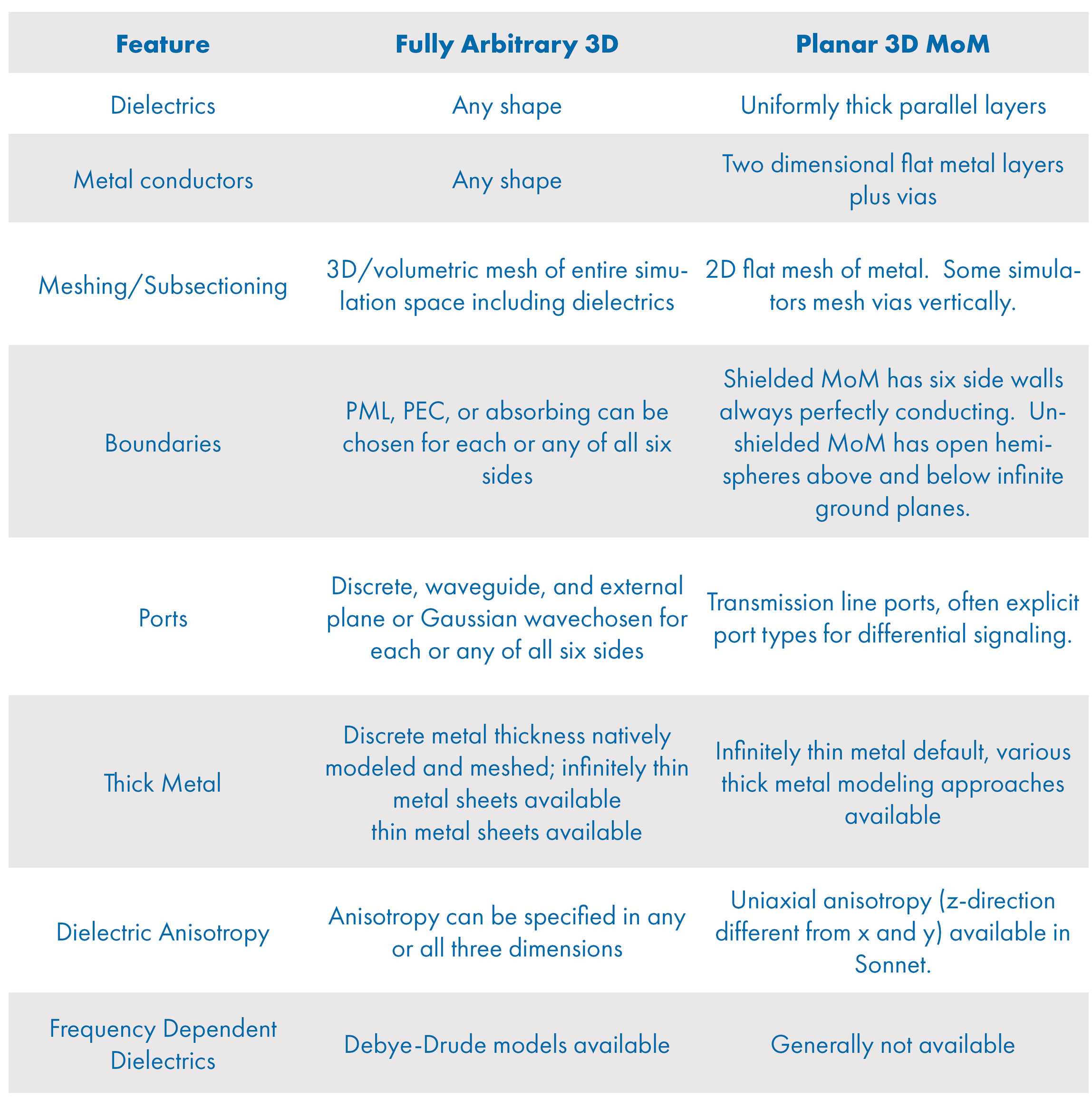
Table 2: Feature comparison between fully arbitrary 3D and planar 3D MoM
References:
“Microwave Circuit Modeling Using Electromagnetic Field Simulation” by Daniel G. Swanson and Wolfgang J.R. Hoefer, Artech House copyright 2003 ISBN: 1-58053-308-6
“The Finite Different Time Domain Method for Electromagnetics” by Karl S. Kunz and Raymond J. Luebbers CRC Press copyright 1993 ISBN: 0-8493-8657-8


