 Summary:
This whitepaper demonstrates how XFdtd's time-domain EM simulation enables rapid development by allowing engineers to determine the performance of a fully detailed sensor model installed behind a piece of fascia without needing to build prototypes and run tests in an anechoic chamber. The analysis of a 25 GHz sensor frames the discussion.
Learn more about WaveFarer Automotive Radar Simulation software...
Trends in automotive safety are pushing radar systems to higher levels of accuracy and reliable target identification for applications like blind spot monitoring and cross traffic alert. Consequently, the requirements for automotive radar sensors in frequency bands such as 24 GHz and 77 GHz are becoming more stringent and engineers need to better understand how design decisions affect performance. Time-domain electromagnetic simulation promotes rapid development by allowing engineers to determine the performance of a fully detailed sensor model installed behind a piece of fascia without needing to build prototypes and run tests in an anechoic chamber. In this article, the analysis of a 25 GHz sensor will be discussed using Remcom’s XFdtd® Electromagnetic Simulation Software (XF).
Analysis of RF Board
The RF board – a multilayer PCB containing the feeding structure and radiating elements – is crucial to the design of any sensor because it is the starting point for target identification. Given its importance, engineers need a tool that helps them understand which structures drive its performance.
Often created in tools from Cadence® or Mentor Graphics®, these boards contain hundreds of traces, vias, and surfaces that are imported into XF as CAD files. Figure 1 shows the details of the four layers in the RF board after import. This board is 88.5 mm x 57 mm x 1.4 mm, contains 188 objects, and has microstrip structures as small as 0.22 mm.
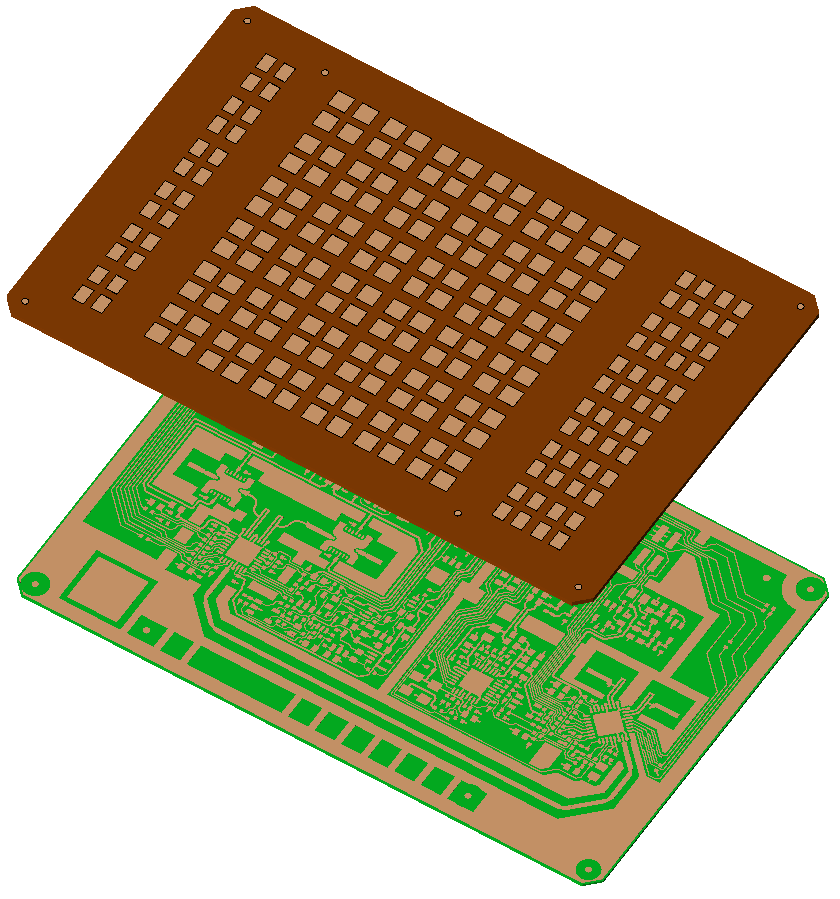
Figure 1: Top and bottom layers of RF board
A simulation of the RF board will generate the same results that can be obtained from measurements: broadband S-Parameters or far-field gain and directivity. As a design tool, these system-level results are not very informative. They are used to compare one design against another or determine if a design meets its requirements.
A design engineer needs more than the standard system-level results in order to understand a device and improve its design. XF can also compute:
-
Parasitic coupling between conductors. S-Parameters and images of frequency domain currents will confirm that parasitic coupling exists, but they do little to identify and fix the problem. Time-domain simulation results generated using the Finite-Difference Time-Domain (FDTD) method allow engineers to see where the coupling occurs and redesign the layout to prevent it.
-
Current distribution on ground planes. At 25 and 77 GHz, grounding structures are no longer equipotential surfaces. As seen in Figure 2, the ground plane has strong currents – 10dB below the maximum – on its edges that need to be considered during the design.
-
Effects of secondary sources like the local oscillator (LO) line. Secondary sources can couple onto other conductors and even generate unintended radiation. Both of these problems can be identified and quantified through simulation.
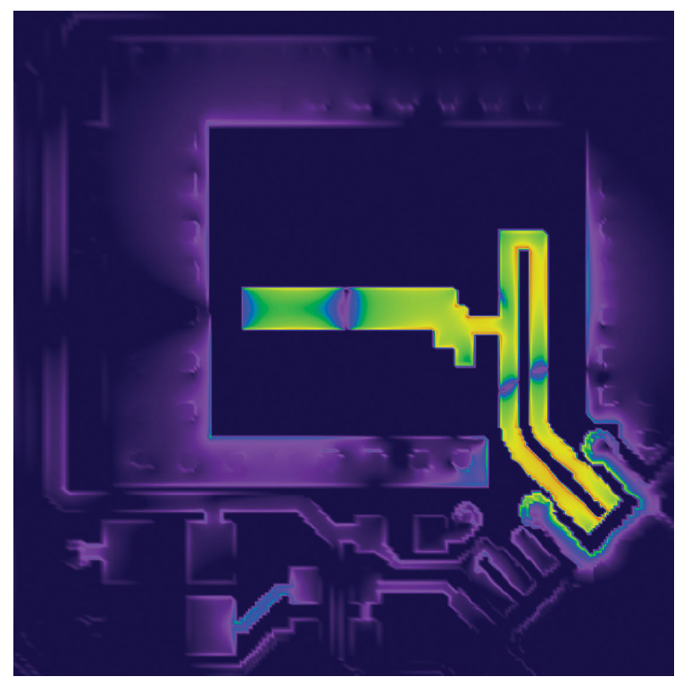
Figure 2: Grounding structures are not equipotential surfaces
Analysis of RF Board with Sensor
A properly designed RF board is an indicator of future success, but there is more work to do before OEM specifications are met. For starters, the RF board needs to be placed in the sensor’s case and covered by a radome. These structures will change the performance of the antenna.
An expanded view of the full sensor model is shown in Figure 3. The model contains the radome, RF board, digital board, packaging, data connector, and sensor case which bring the overall dimensions to 106 mm x 63 mm x 21 mm.
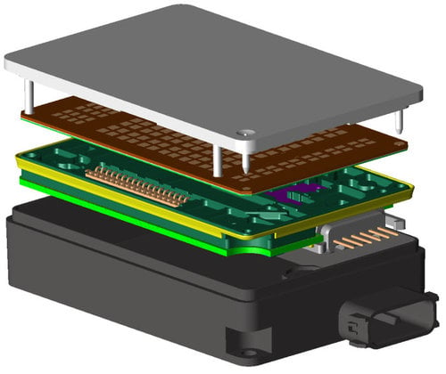
Figure 3: Expanded view of full sensor
An FDTD simulation includes all of the model’s complexity so no simplifications to the sensor are needed. This gives engineers a more realistic picture of how the sensor will perform if it is built. For example, the data connector is a relatively large structure that is not in the immediate proximity of the radiators so one may remove it from the simulation to reduce RAM requirements. Including it in the simulation, however, increases accuracy because energy couples onto its pins and is then radiated from these dipole-like structures.
The radome is one of the most important structures of the sensor because it sits directly in front of the antenna arrays and can have a large impact on the antenna’s radiation patterns. By parameterizing the imported radome model, its design can be honed to meet the desired performance. The results from a basic parameter sweep of the radome thickness are shown in Figure 4. Parameterizing the geometry and setting up the simulations can be accomplished in minutes, which is significantly less than the time it would take to create and measure five different radomes in a lab.
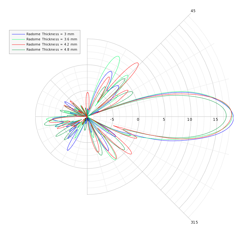
Figure 4: Far-field gain results for different radome thicknesses
Analysis of Sensor Behind Fascia
Ultimately, the installed sensor’s performance will dictate the sensor’s ability to accurately identify targets. Here, engineers are interested in understanding how mounting brackets, paint color, and curves in the fascia will degrade the antennas’ radiation pattern.
Models of fascia, obtained from an OEM, can be imported into XF like any other CAD model. Figure 5 shows an example of a fascia model included with the sensor. The corresponding simulation space is 195 mm x 204 mm x 74 mm.
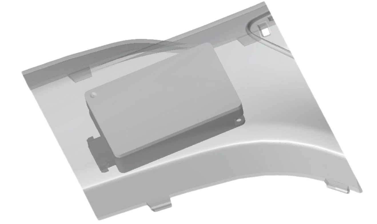
Figure 5: Sensor mounted behind fascia
Application and design engineers benefit from simulation because it allows them to identify the optimal placement of a sensor behind a fascia or troubleshoot problems with an installation. Similar to parameterizing the radome’s thickness, the sensor’s location relative to the fascia can be parameterized. This, coupled with the ability to visualize trapped modes between the radome and fascia, allow engineers to understand which aspects of the installation are impacting the results.
Run Time and Memory Requirements
The ability to complete simulations in a timely manner is an important factor in determining the usefulness of a simulator. Combining graphics processing unit (GPU) technology and FDTD allows engineers to perform multiple design iterations much faster than previously possible.
The chart in Figure 6 compares the memory requirements and run time for three simulations: RF board only, RF board with full sensor, and sensor with fascia. The microstrip structures in the RF board generated a minimum cell size of 0.037 mm and the grid definition around the RF board was maintained as the problem size grew with the additional geometry. For the benchmark, XF utilized four NVIDIA® GPUs with the Kepler architecture.
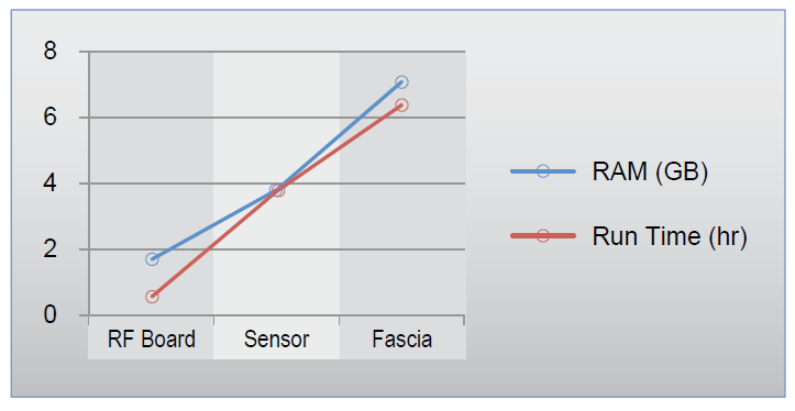
Figure 6: Run time and memory requirements
GPUs provide a massively parallelized computing platform with 2,800 cores per card. The FDTD algorithm efficiently utilizes this parallelization and 50x speed improvements over CPUs are commonly achieved. This combination enables full sensor with fascia simulations to complete in under seven hours.
Summary
Engineers are pushing the limits of sensor technology in order to meet OEM requirements and improve transportation safety. FDTD simulation provides the tools they need to understand an antenna’s performance. At the board level, sources of parasitic coupling or variations in ground potential can be identified and mitigated. This type of analysis carries through to optimizing radome structures and determining the best location for a sensor behind a fascia. Coupled with GPU technology, engineers are able to perform this analysis in hours, thus reducing the overall development time.