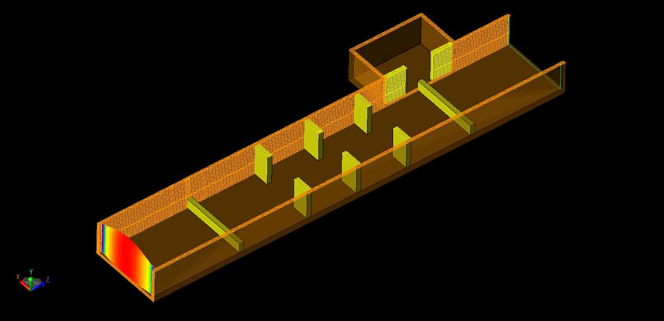
This example describes the simulation of a waveguide filter that includes both E- and H-plane cavity-backed inverters in addition to several irises [1]. The basic geometry is shown in CAD format in Figure 1 where the E-plane cavity-backed inverter is above the waveguide and the H-plane cavity-backed inverter is on the back side. The waveguide is WR-90 and the dimensions of the design including the spacing and dimensions of the cavities and irises are easily entered as parameters into the XFdtd model. The structure is meshed with a 0.4 mm base cell size and fixed points are used on all parts to ensure the FDTD grid lines overlap the CAD dimensions.
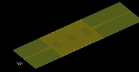
The input port has a fundamental mode applied as shown in the cut-away mesh view of Figure 2. The frequency for the input excitation is 12 GHz which ensures frequency content in the simulation over the 8 to 12 GHz range of the device. The output for the simulation will be the S-parameters at the input and output ports, some images of the transient electric field propagation though the device, and point sensors of the electric field versus time.
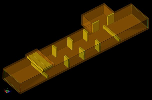
Figure 1: CAD representation of the device as constructed in XFdtd.
The simulation requires approximately 122 MB of computer memory and runs to -45dB convergence in just over 14 minutes on an NVIDIA C1060 Tesla GPU card.
Following the simulation, the resulting S-parameters at each port, shown in Figure 3, are found to be a good match to the measured values reported in the paper. The transient electric field at an instance in time through the cross-section of the filter is shown in Figure 4. The transient electric field at point locations centered just beside each of the ports is shown in Figure 5.
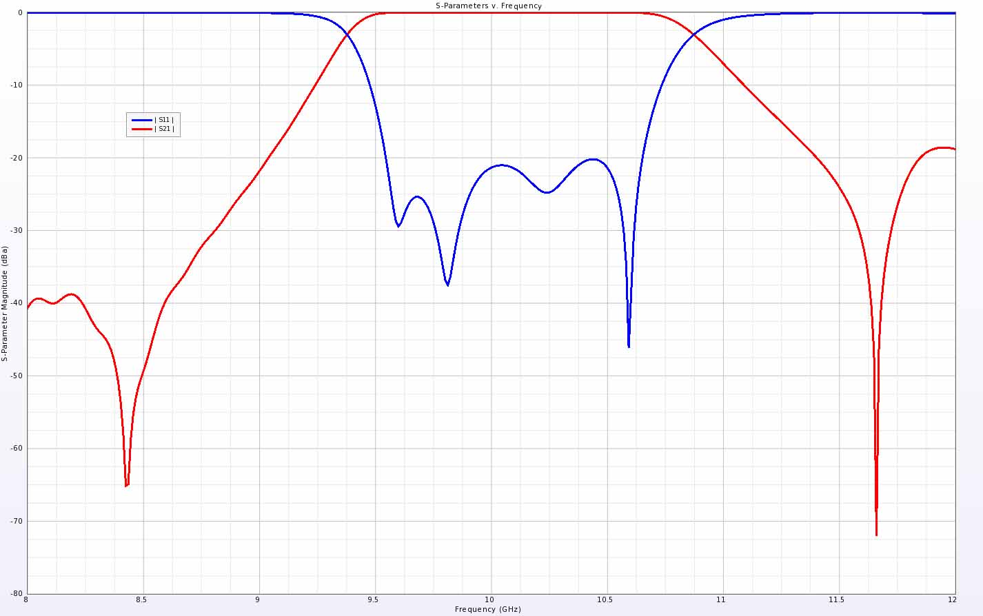
Figure 3: Resulting S11 and S21 of the device as simulated in XFdtd.
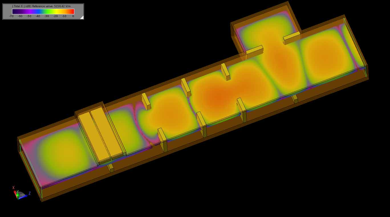
Figure 4: Transient electric fields propagating in the filter.
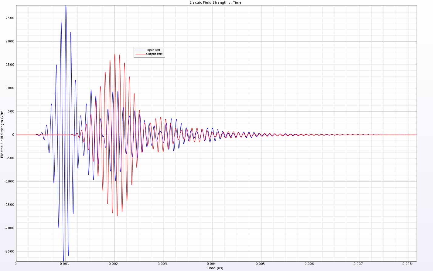
Figure 5: Electric field point sensor at the input and output ports of the filter.
References
-
Q. F. Zhang and Y. L. Lu, “Design of Wide-Band Pseudo-Elliptic Waveguide Filters With Cavity-Backed Inverters,” IEEE Microw. and Wirel. Comps. Letters, Vol. 20, Nov. 2010, pp. 604-606.