Introduction
In this example, XFdtd is used in an antenna simulation focused on the performance of a substrate integrated waveguide (SIW) leaky wave antenna with transverse slots. The design was taken from the paper by Liu, Jackson, and Long [1]. The antenna operates like a transverse slotted rectangular waveguide, but is designed in SIW for reduced cost, size, and for easier integration with planar circuits. Results for S-parameter performance, antenna gain, and efficiency are computed.
Device Design and Simulation
A top view of the entire antenna is shown in Figure 1 where the green material represents copper and the red is a dielectric (relative permittivity = 2.25 and loss tangent of 0.001). The device is approximately 310 mm in length, 40 mm in width, and 1 mm in height. The copper microstrip layer at the top of the antenna has transverse slots spaced at regular intervals and tapered at the ends. At each end of the device a nodal waveguide port is connected to a tapered microstrip line that connects to the SIW portion. In the top layer are a number of transverse slots, more easily seen in Figure 2. The edges of the top microstrip layer are terminated with vias. The layers are shown in angled views in Figures 3 through 5 where all parts are shown in Figure 3, the substrate is visible in Figure 4, and the vias in Figure 5.

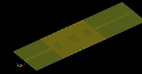
Figure 1: A top view of the 3D CAD model of the antenna shows input and output ports at the ends attached to tapered microstrip lines and a center microstrip section with numerous slots.

Figure 2: A detailed view of one end of the antenna shows the tapered slots and the curved via path located under the microstrip line.
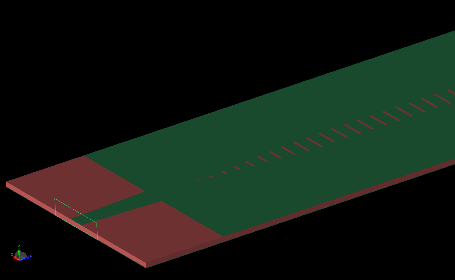
Figure 3: An angled view of the antenna from one port shows the nodal waveguide port attached to the tapered line, the thickness of the substrate layer, and a portion of the slotted top layer.
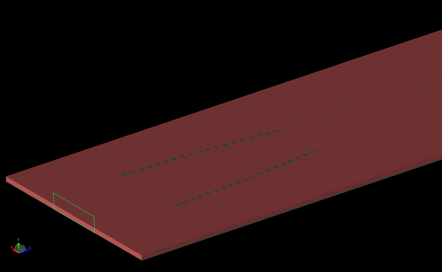
Figure 4: With the top microstrip layer removed, the substrate and some of the vias are visible in the antenna structure.
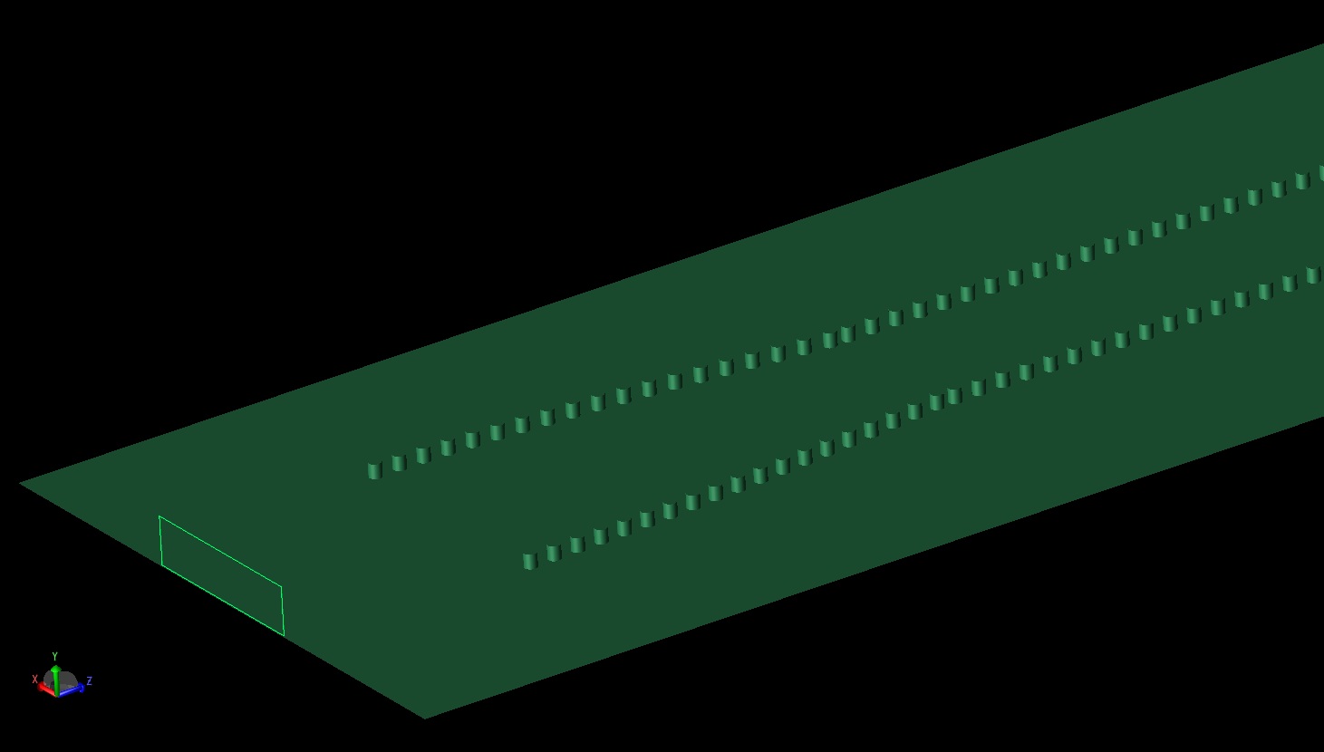
Figure 5: In this figure the substrate layer has been removed and the ground plane and vias are visible.
The device is simulated by applying a frequency-limited signal to the waveguide port at one end. The S-parameter results are shown in Figure 6 and it can be seen that the device has good operating performance from 10.4-12.5 GHz and a few smaller frequency bands below 10.4 GHz. Below 10 GHz the response is cutoff.
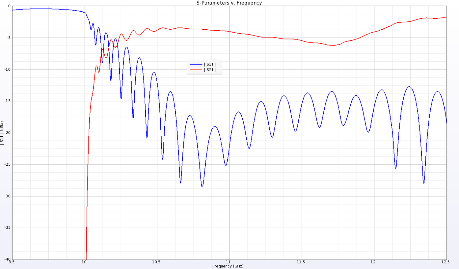
Figure 6: The S-parameters show good return loss from about 10.4 GHz up to 12.5 GHz while the S21 has between -6 to -2 dB of loss in the same region.
The antenna produces several beams which range from near broadside to near end fire depending on the frequency. These beams are generally narrow and fan-shaped. At 10.2 GHz, the beam is quite narrow and peaks at about 8.6 dBi at theta=70 degrees in the YZ plane as shown in Figure 7 in a polar plot. The 10.2 GHz pattern is shown as a three-dimensional plot from the same angle as the polar plot of Figure 7 in Figure 8. A different perspective of the 10.2 GHz three-dimensional pattern is shown in Figure 9. At 10.8 GHz, the peak gain increases to 11.1 dBi and the beam shifts to a peak at theta=49 degrees in the YZ plane as shown in Figures 10, 11, and 12. The pattern broadens slightly and increases in peak gain at 11.5 GHz where the main lobe direction changes to theta=28 degrees and the maximum gain is 12.7 dBi as shown in Figures 13, 14, and 15. At 11.7 GHz the maximum gain is 14 dBi at an angle of theta=19 degrees as shown in Figures 16, 17, and 18. Finally, at 12 GHz, the maximum gain is 14.2 dBi at an angle of theta=13 degrees as shown in Figures 19, 20, and 21.
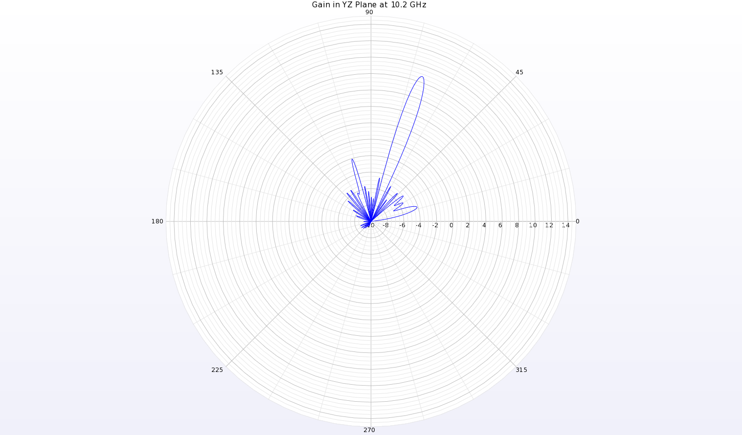
Figure 7: A polar plot of the gain pattern at 10.2 GHz in the YZ plane (along the length of the antenna) shows a narrow beam at theta=70 degrees with a gain of about 8.6 dBi.
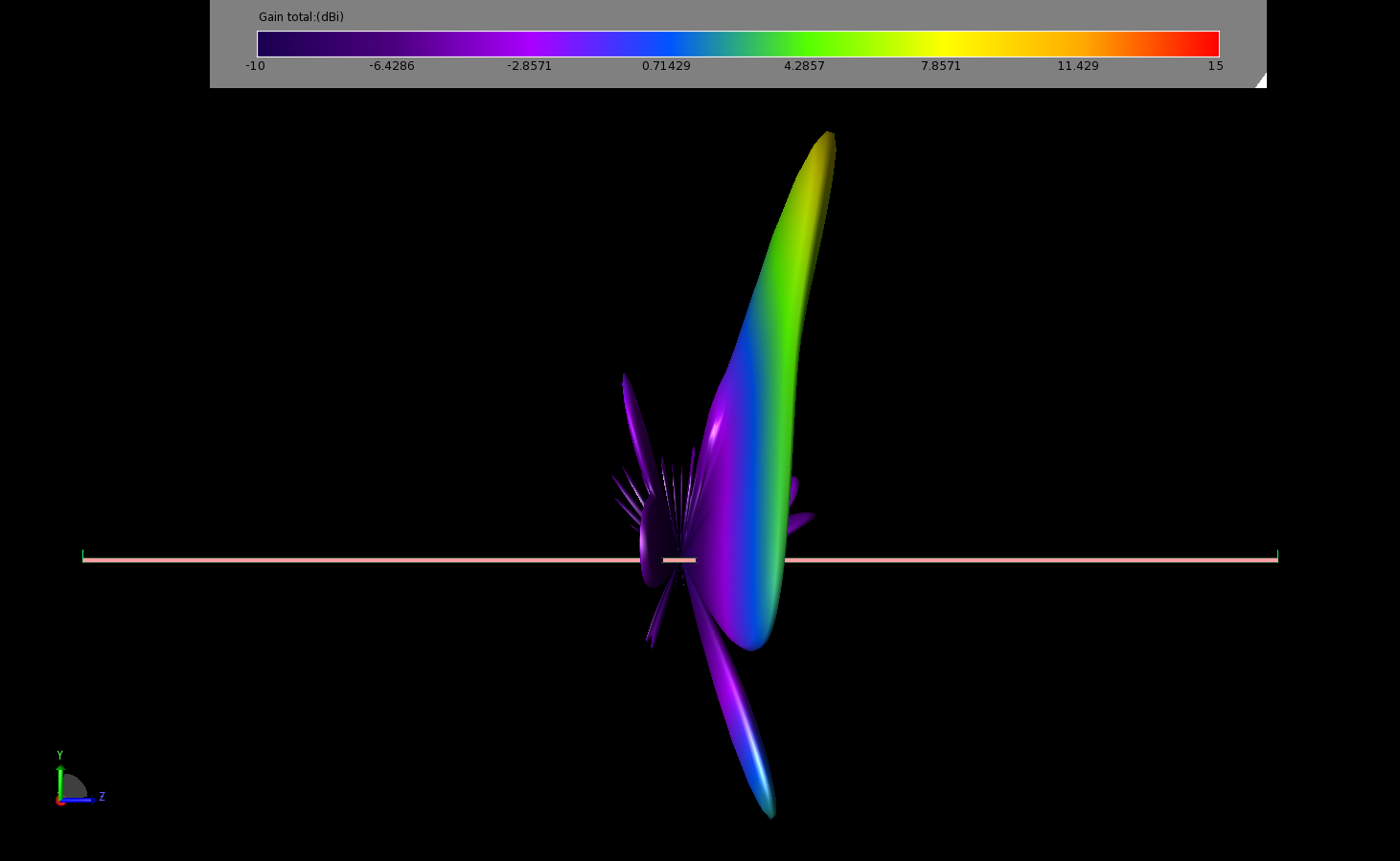
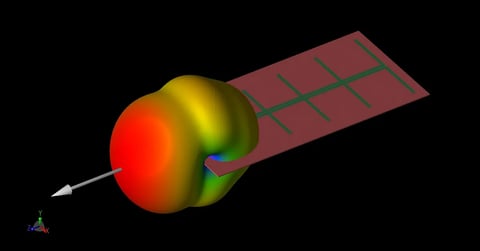
Figure 8: The gain pattern of the antenna at 10.2 GHz is shown here in a three-dimensional view overlaid on the antenna geometry.
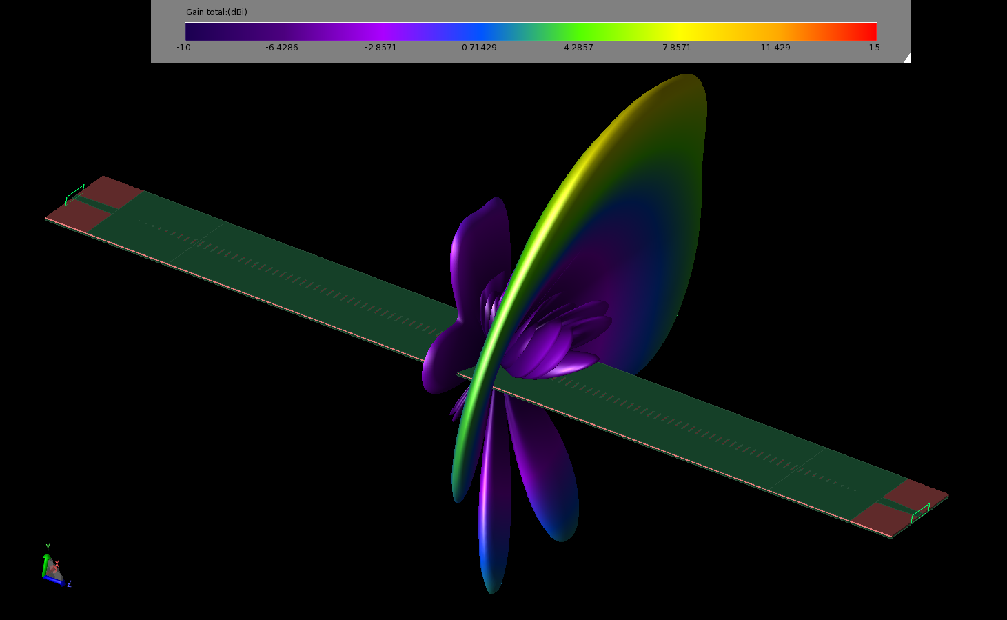
Figure 9: The gain pattern of the antenna at 10.2 GHz is shown from an angled three-dimensional view to demonstrate the fan shape of the pattern.
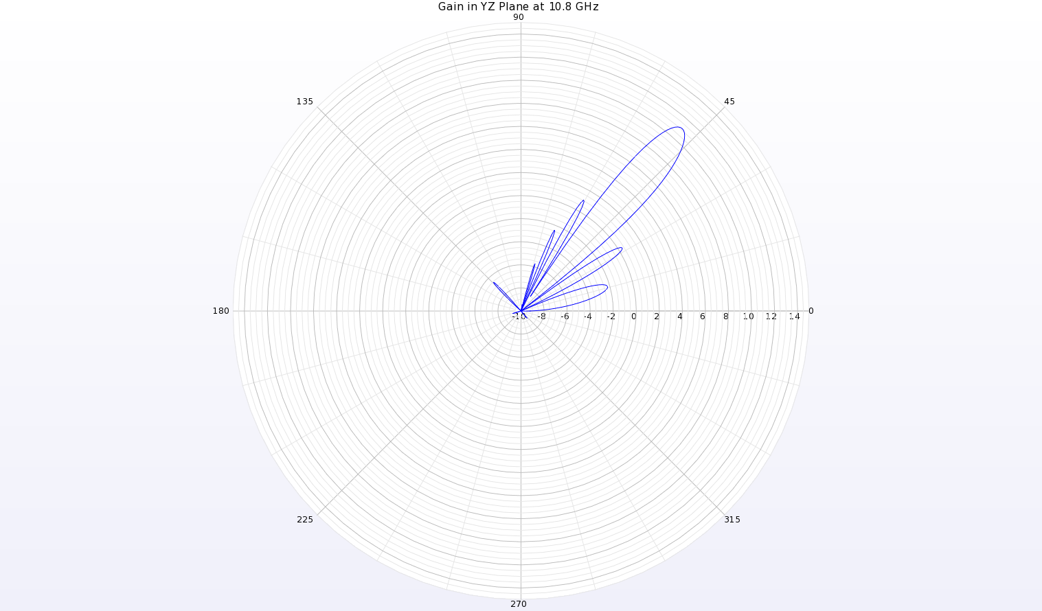
Figure 10: A polar plot of the gain pattern at 10.8 GHz in the YZ plane of the antenna shows a beam at theta=49 degrees with a peak gain of 11.1 dBi.
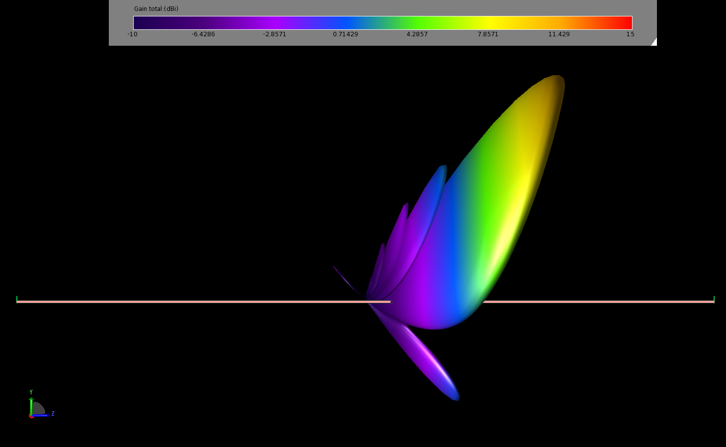
Figure 11: The gain pattern of the antenna at 10.8 GHz is shown here in a three-dimensional view overlaid on the antenna geometry.
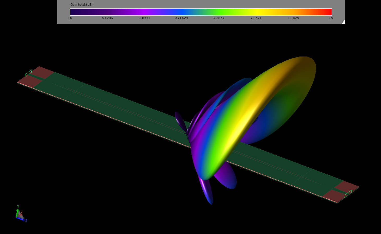
Figure 12: The gain pattern of the antenna at 10.8 GHz is shown from an angled three-dimensional view to demonstrate the fan shape of the pattern.
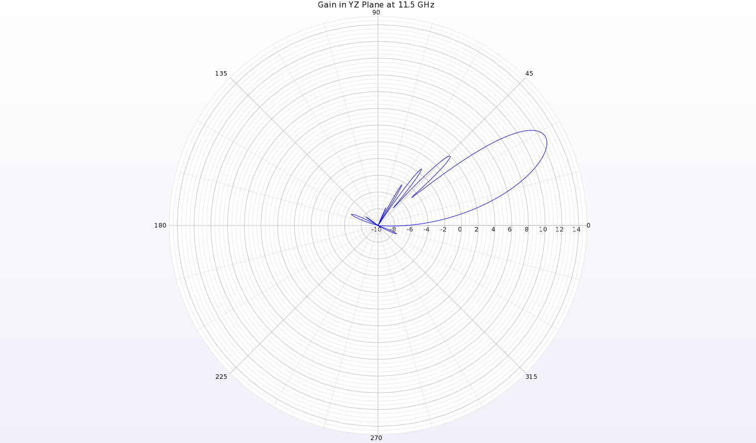
Figure 13: A polar plot of the gain pattern at 11.5 GHz in the YZ plane of the antenna shows a beam at theta=28 degrees with a peak gain of 12.7 dBi.
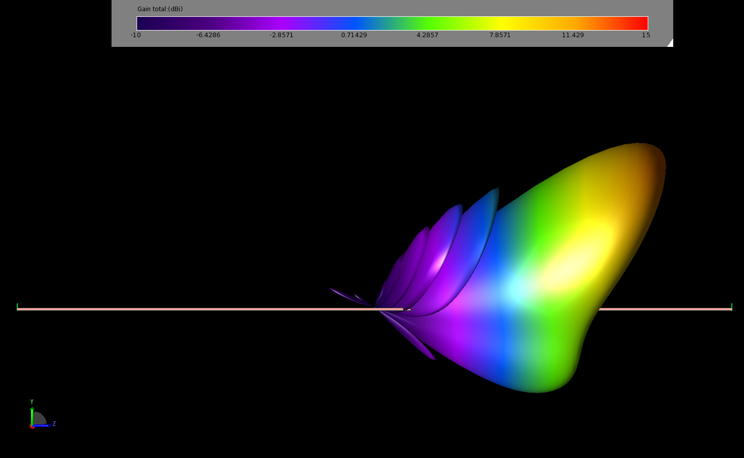
Figure 14: The gain pattern of the antenna at 11.5 GHz is shown here in a three-dimensional view overlaid on the antenna geometry.
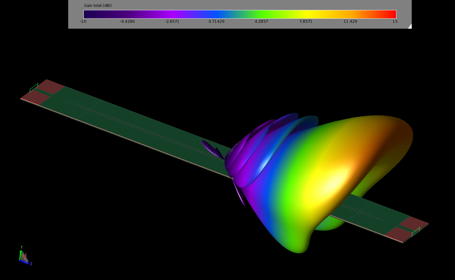
Figure 15: The gain pattern of the antenna at 11.5 GHz is shown from an angled three-dimensional view to demonstrate the fan shape of the pattern.
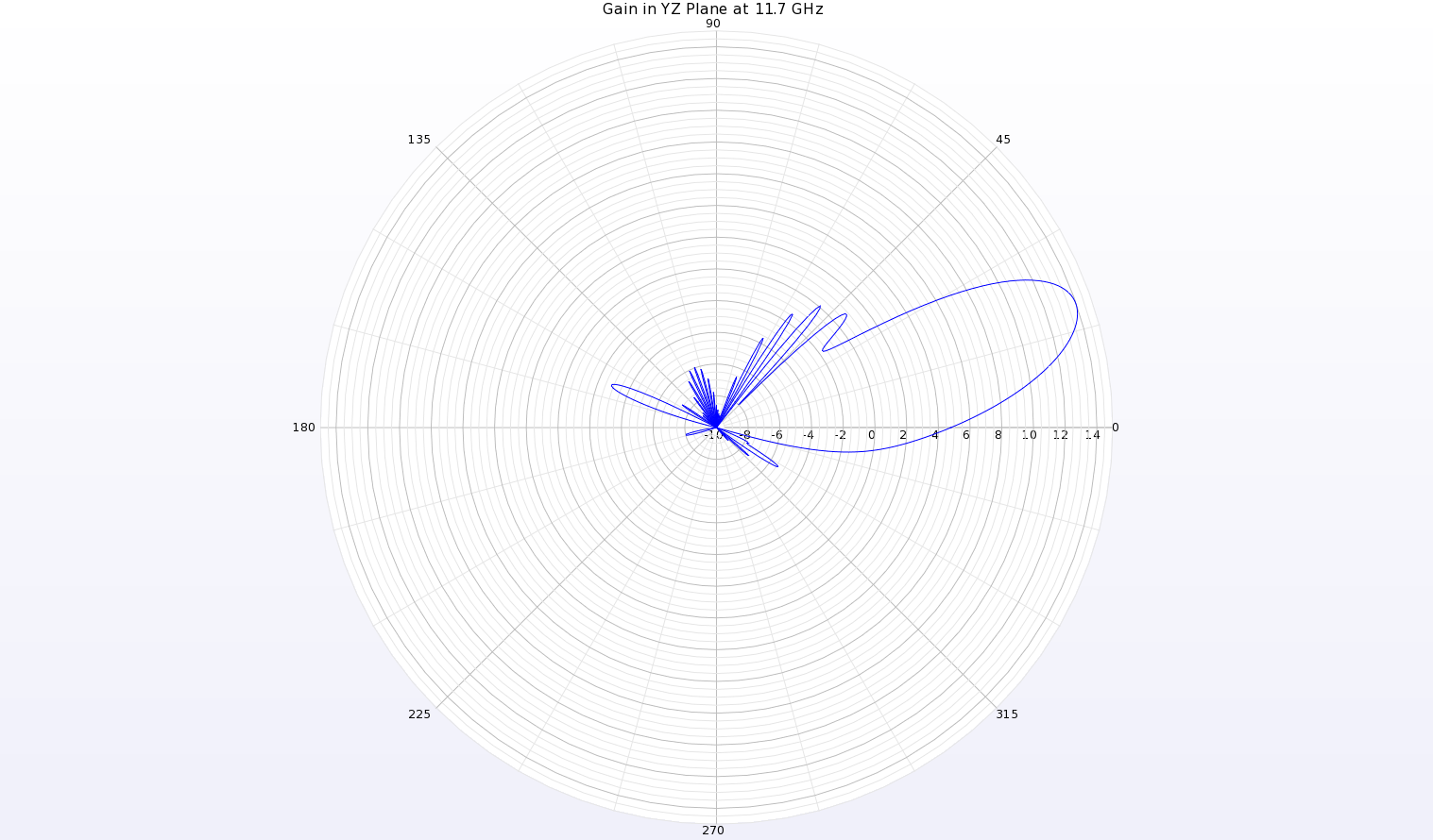
Figure 16: A polar plot of the gain pattern at 11.7 GHz in the YZ plane of the antenna shows a beam at theta=19 degrees with a peak gain of 14 dBi.
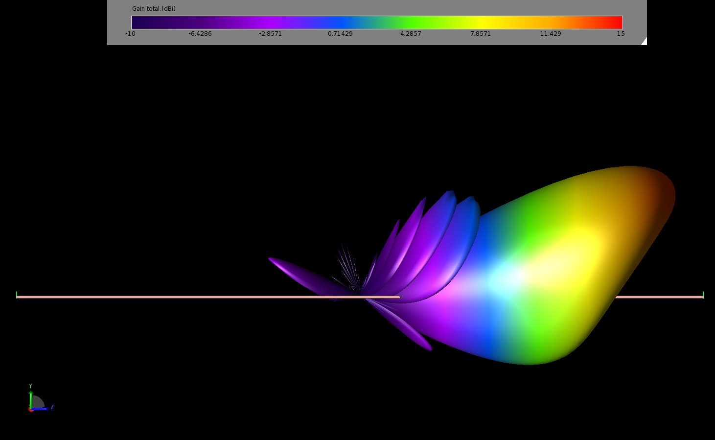
Figure 17: The gain pattern of the antenna at 11.7 GHz is shown here in a three-dimensional view overlaid on the antenna geometry.
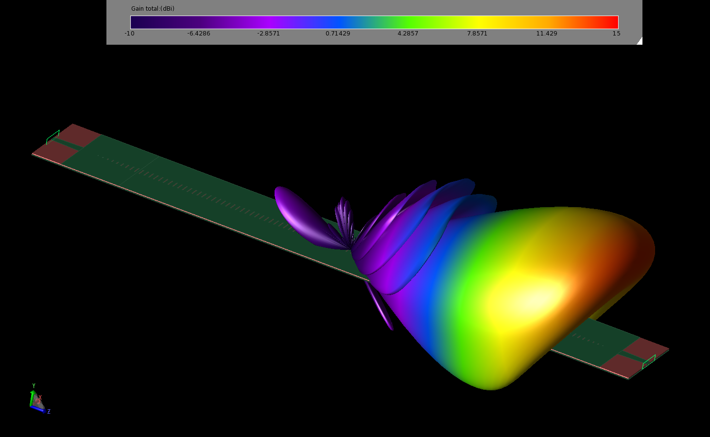
Figure 18: The gain pattern of the antenna at 11.7 GHz is shown from an angled three-dimensional view to demonstrate the fan shape of the pattern.
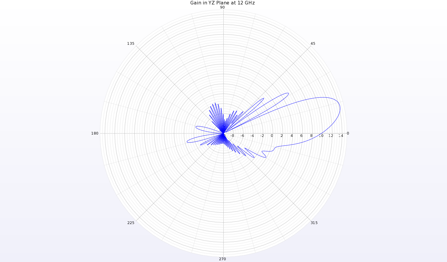
Figure 19: A polar plot of the gain pattern at 12 GHz in the YZ plane of the antenna shows a beam at theta=13 degrees with a peak gain of 14.2 dBi.
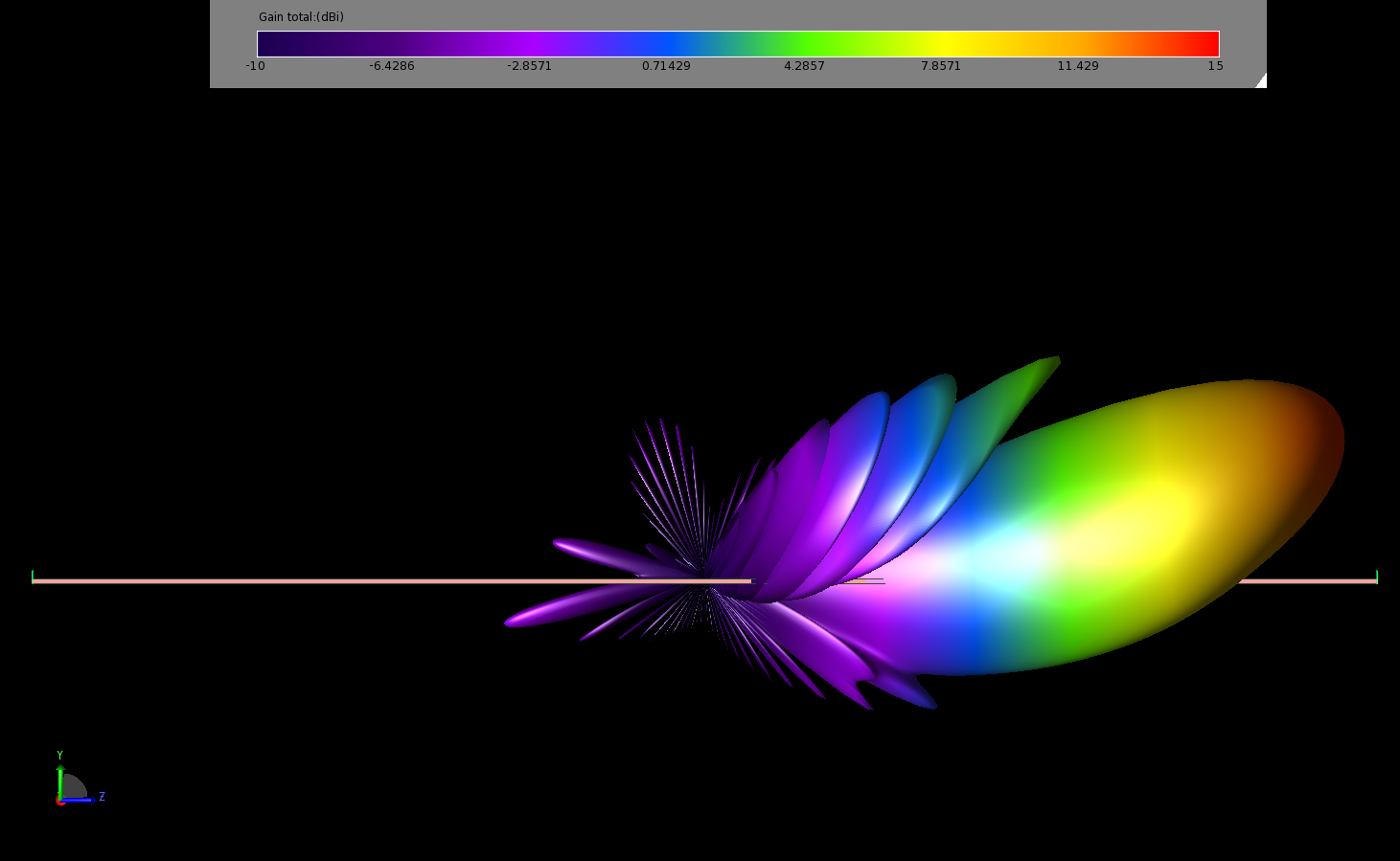
Figure 20: The gain pattern of the antenna at 12 GHz is shown here in a three-dimensional view overlaid on the antenna geometry.
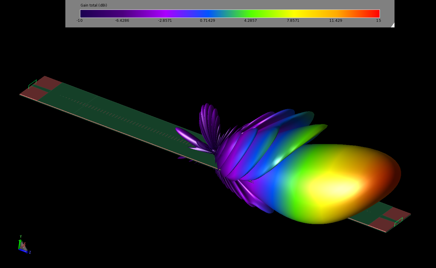
Figure 21: The gain pattern of the antenna at 12 GHz is shown from an angled three-dimensional view to demonstrate the fan shape of the pattern.
The radiation efficiency is computed in the paper using a theoretical approach for a slotted rectangular waveguide which does not consider the system mismatch or the power lost in other ports. A value comparable to this theoretical one is computed in XFdtd and is labeled the standalone radiation efficiency. The theoretical radiation efficiency from the paper is plotted in Figure 22 along with the standalone radiation efficiency from the XFdtd 3D EM simulation software and the XFdtd system efficiency, which includes both the mismatch loss and the power lost in the second waveguide port.
![Figure 22: Shown is the radiation efficiency for the antenna. The theoretical result from the paper [1] is for a slotted rectangular waveguide. The XFdtd results are for the system efficiency which includes the mismatch loss and loss in the second p…](https://www.remcom.com/hubfs/Imported_Blog_Media/image-asset-Apr-03-2023-08-59-32-6122-PM.png)
Figure 22: Shown is the radiation efficiency for the antenna. The theoretical result from the paper [1] is for a slotted rectangular waveguide. The XFdtd results are for the system efficiency which includes the mismatch loss and loss in the second port, and the standalone efficiency which is only for radiation and does not include other losses.
Summary
This example has demonstrated the performance of a leaky wave antenna implemented on a slotted substrate integrated waveguide. The antenna produces narrow beams that scan from near broadside to endfire as the frequency increases. The antenna has a wide impedance bandwidth and efficiency that improves with an increase in the operating frequency.
Reference:
[1] J. Liu, D. R. Jackson, and Y. Long, “Substrate Integrated Waveguide (SIW) Leaky-Wave Antenna With Transverse Slots,” IEEE Trans. Antennas Propag., vol. 60, no. 1, pp. 20-29, Jan. 2012.