In this example a 9-pin connector is imported into XFdtd from an SAT (saved-as-text) CAD file, a standard format file. The connector is comprised of three main parts: the conducting outer package, the 9-pins (male and female) that form the connection, and the insulating dielectric surrounding the pins. The full connector assembly is shown in Figure 1 where the conducting parts are displayed in white and the dielectric in green. In Figure 2 the outer package has been removed to show the dielectric insulators and the ends of the pins. Figure 3 shows the pins only.
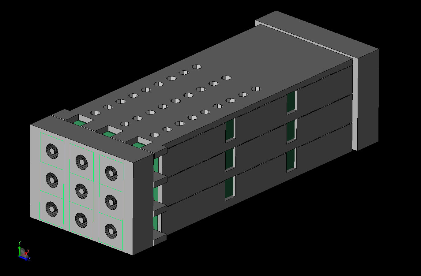
Figure 1: CAD view of the entire connector with all parts visible.
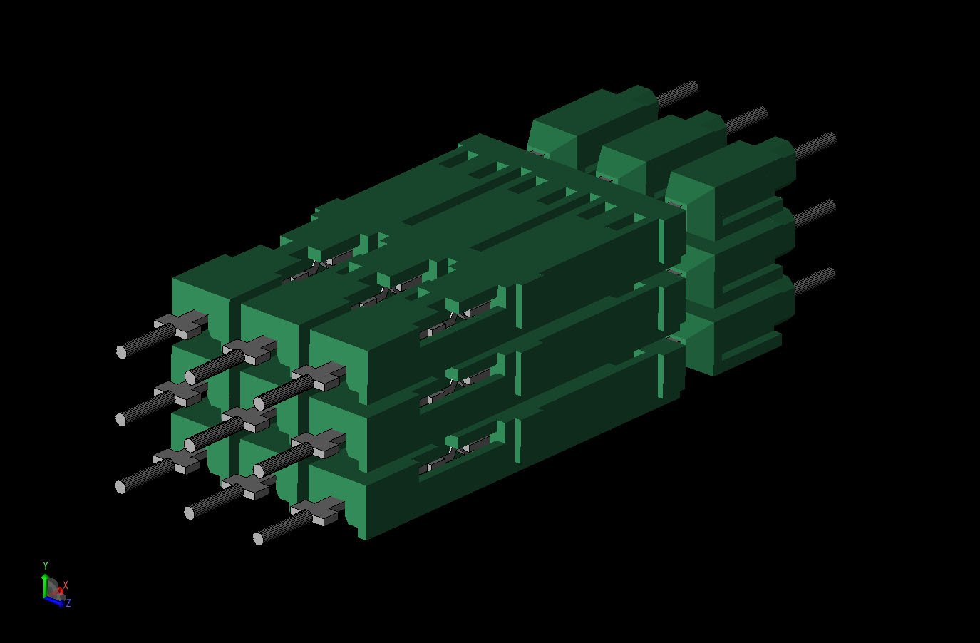
Figure 2: CAD view of the connector with the external shield removed showing the internal pins and insulation.
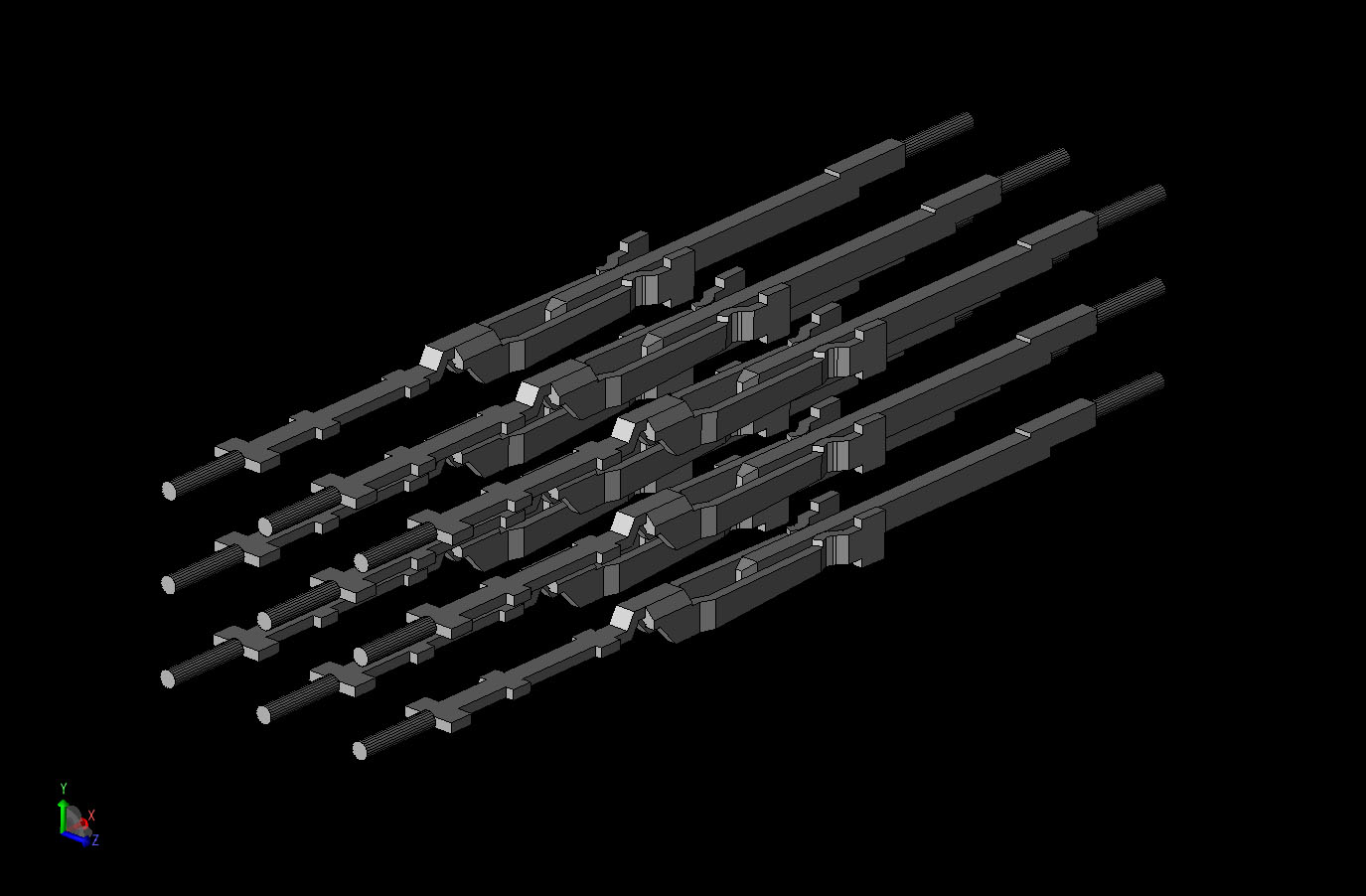
Figure 3: CAD view of the connector with only the pins visible. As can be seen, the pins meet in the center in male and female parts.
Due to the high level of detail, the device is meshed in an FDTD grid at a 0.075 mm resolution producing a geometry of about 13 million cells. A view of the resulting mesh is shown in Figure 4 where several parts have been removed to show the details of the internal components.
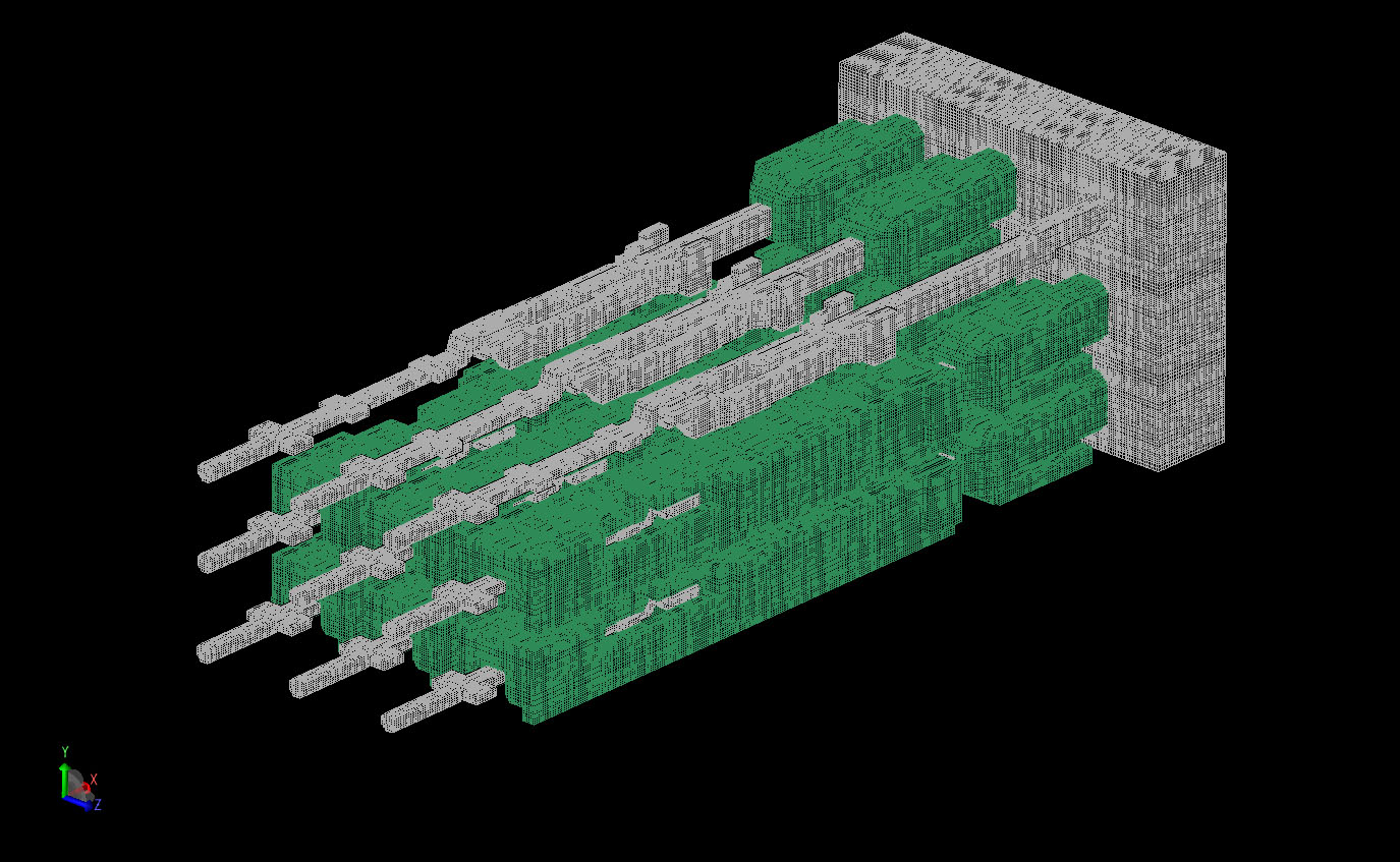
Figure 4: Mesh view of the FDTD geometry in XF7 with some parts removed to show internal detail.
The excitation for the simulation will be a broadband Gaussian pulse with frequency content up to 10 GHz. The pulse is fed into one of the pins using the waveguide port feature of XFdtd. The resulting field distribution of the input port is shown in Figure 5. For this simulation, the signal will be applied to the pin in the bottom right corner of Figures 1-4 with the input entering from the +X side of the pin with propagation toward the -X end. The S-parameters at all pins will be stored for this simulation.
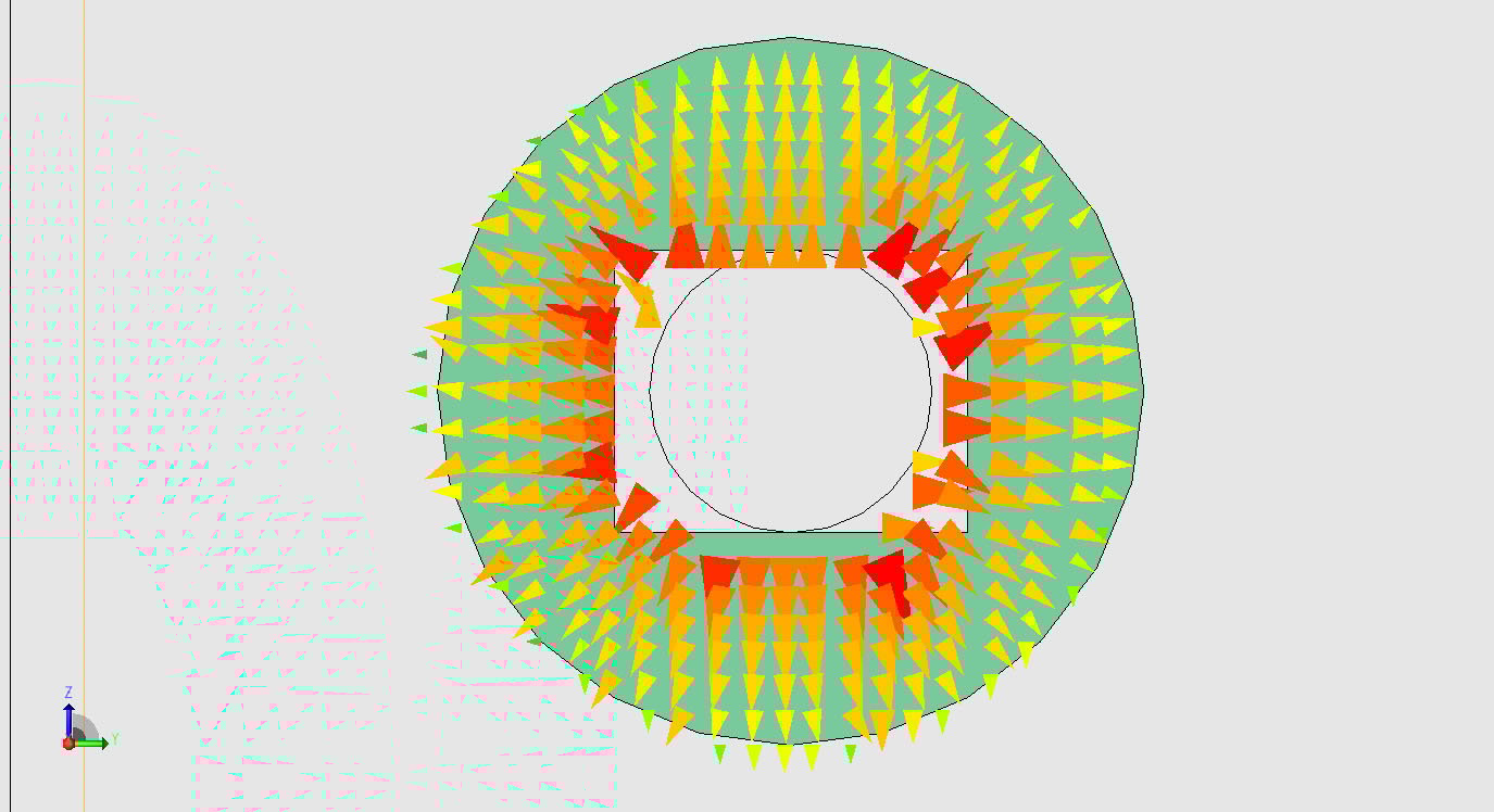
Figure 5: The input port field distribution used to excite the simulation using the waveguide port feature.
In Figure 6 the electric field on the excited pin is shown at a point where the signal is just reaching the output end of the pin. By Figure 7, the fields have passed the end of the pin and are starting to flow into the other neighboring pins. In Figure 8, sufficient time has passed for the fields to reach all pins in the structure.
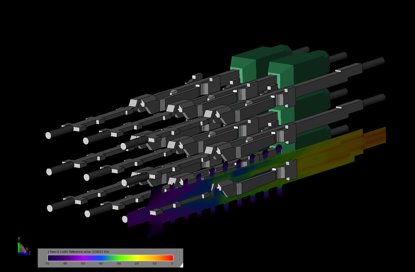
Figure 6: Transient electric field in a cross-sectional cut of the connector as the field is just reaching the output port.
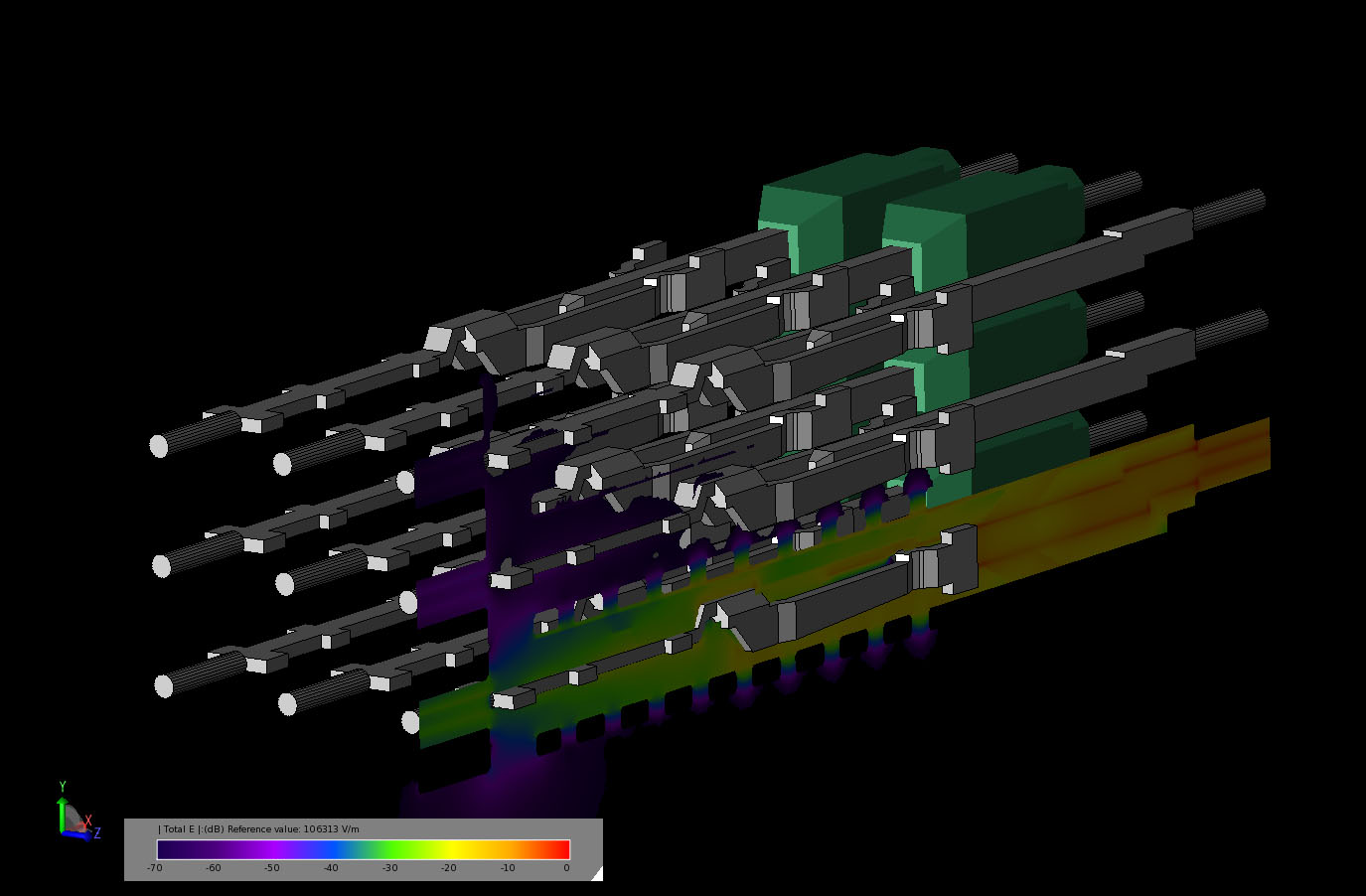
Figure 7: Transient electric field in a cross-sectional cut of the connector as the field is spreading beyond the output port to the adjacent ports.
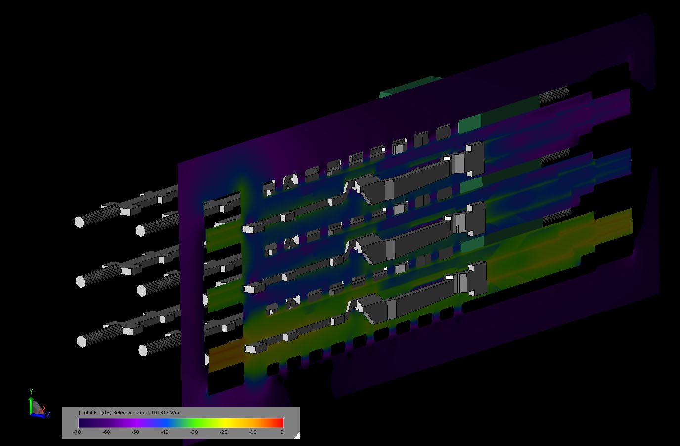
Figure 8: Transient electric field in a cross-sectional cut of the connector after the field has reached all ports in the device.
In Figures 9-11 the electric fields are shown at the same instances in time as displayed in Figures 6-8 but this time in the plane of the output port. As can be seen, the fields on the most distant pin to the output port are about 30 dB down from the peak level present at the output.
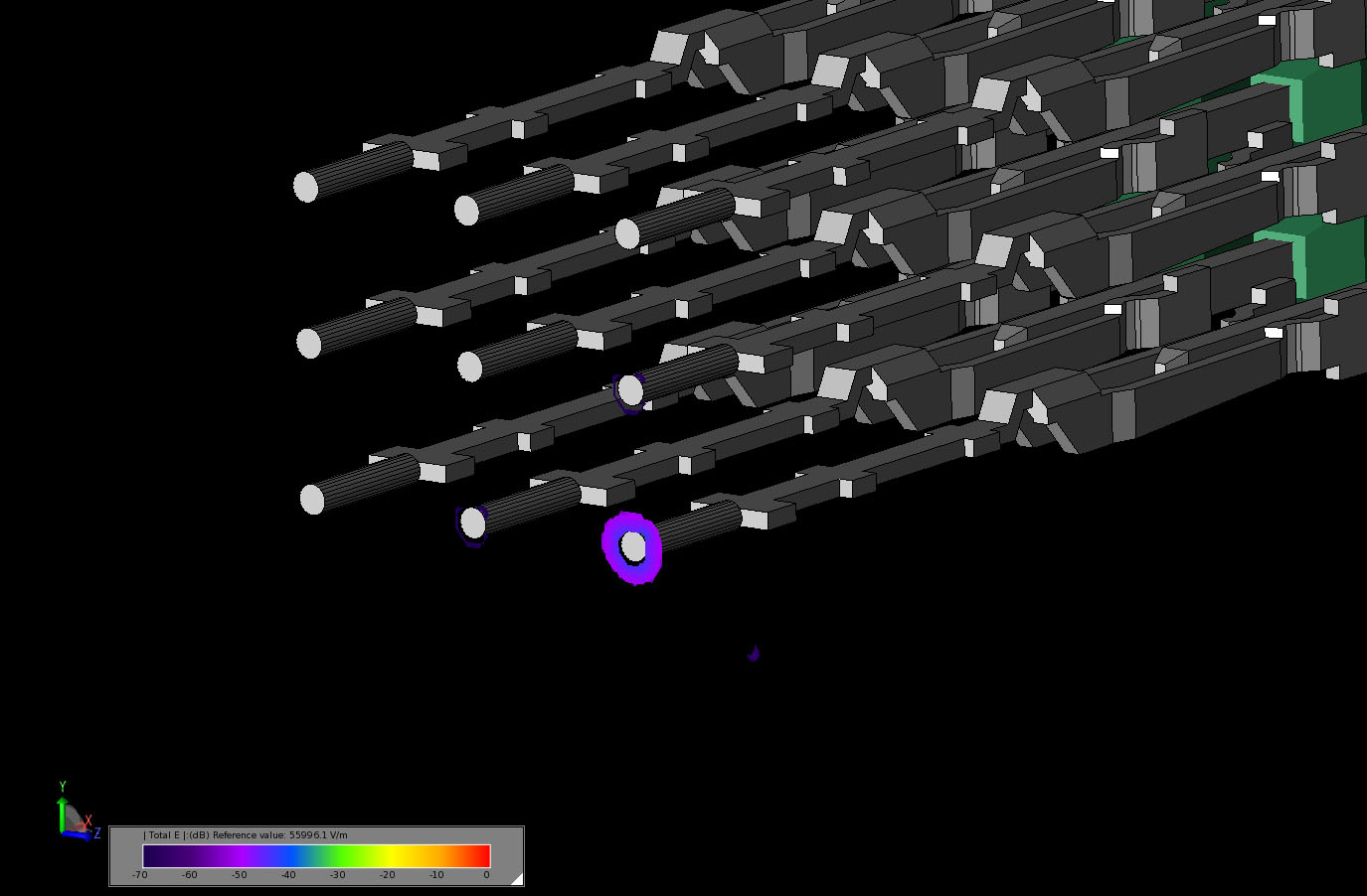
Figure 9: Transient electric field in a cut through the output port plane of the connector as the field is just reaching the output port.
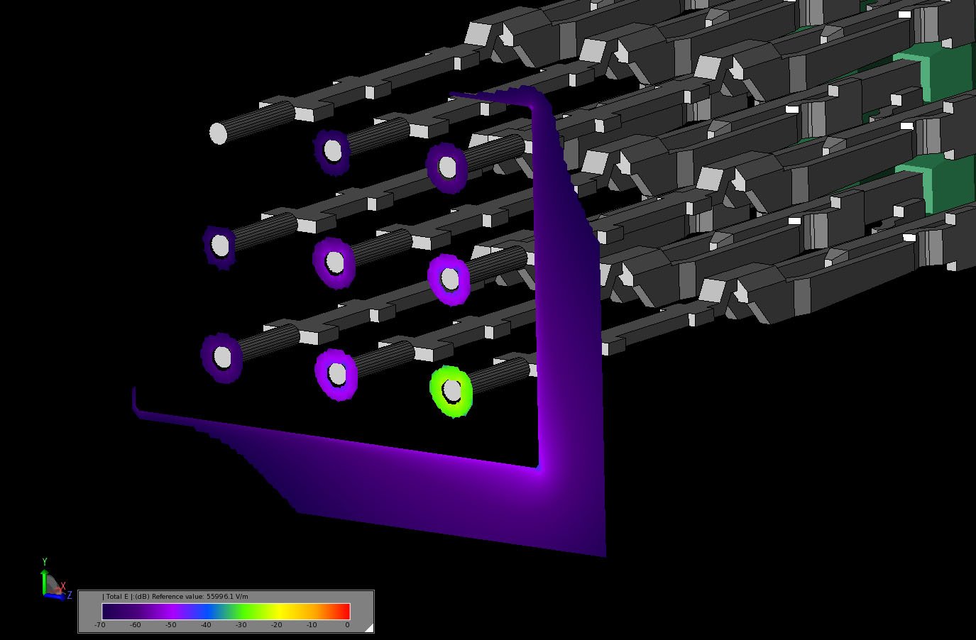
Figure 10: Transient electric field in a cut through the output port plane of the connector as the field is spreading beyond the output port to the adjacent ports.
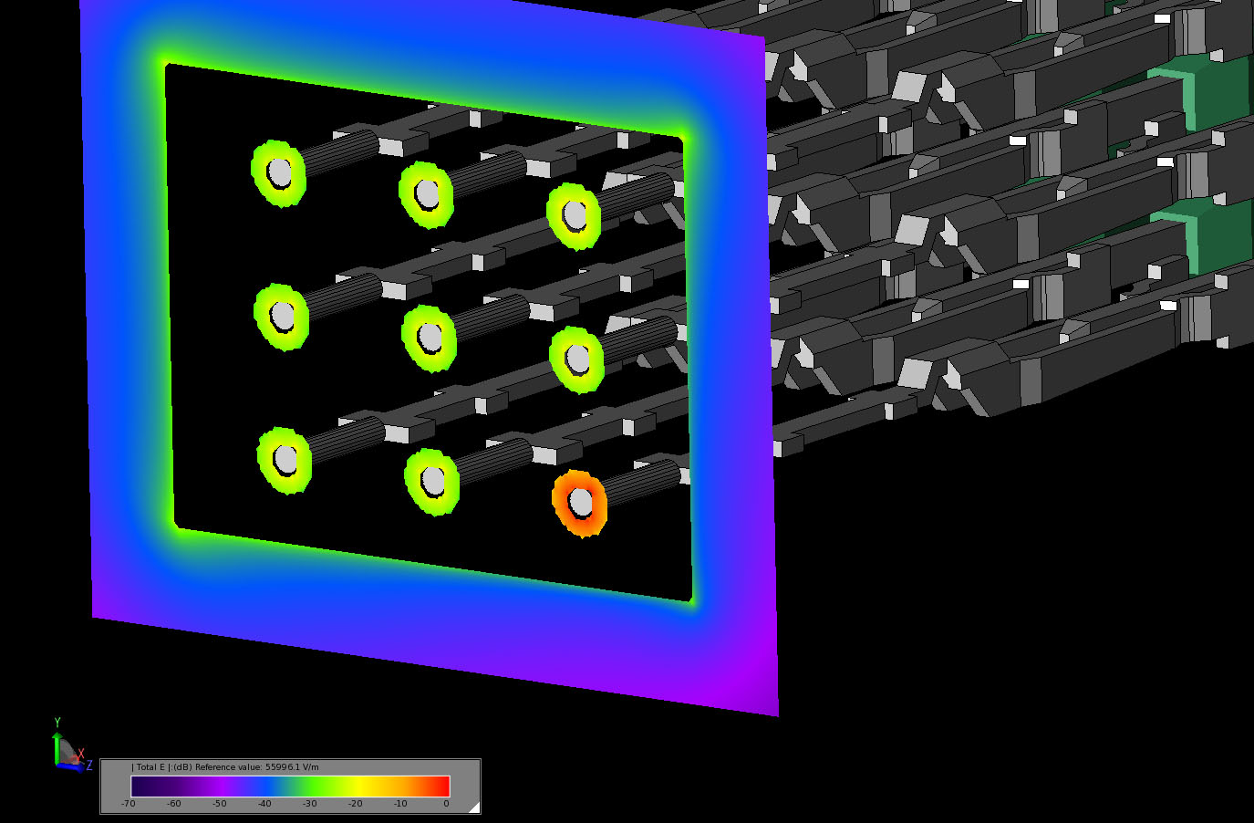
Figure 11: Transient electric field in a cut through the output port plane of the connector after the field has reached all ports in the device.
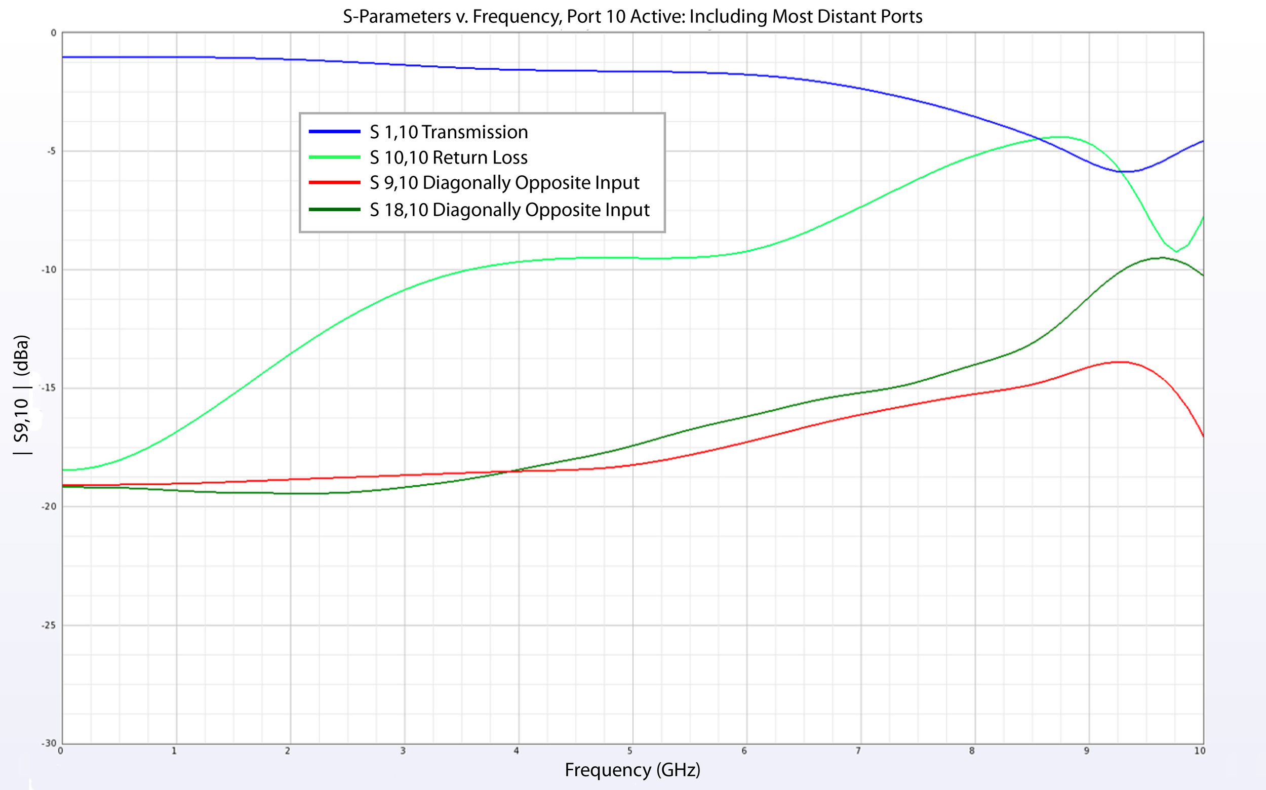
Figure 12 shows the steady state electric fields in three planes of the connector at 2 GHz. The image indicates that the field level at all pins of the structure is about 30 dB down from the peak. In Figure 13 the S-parameters are plotted graphically as a function of frequency. The transmission from input to output shows a loss between 1 and 6 dB over the frequency range. The return loss from the input is low from 0 to 6 GHz and then rises toward the upper end of the frequency band. The cross coupling in the adjacent ports (to the left of the excited pin) show levels down more than 15 dB over the band. For the pin diagonally opposite the excited pin (see Figure 14), the cross coupling is 15 dB out to 6 GHz and then increases at higher frequencies.
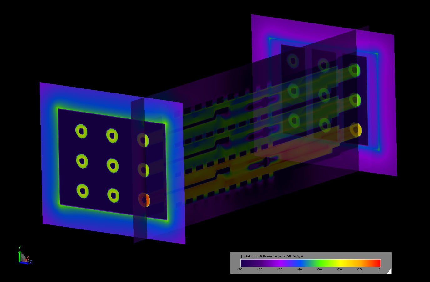
Figure 12: Steady state electric fields in three planes of the connector: through the cross section of the excited pin, through the plane of the output port, through the plane of the input port.
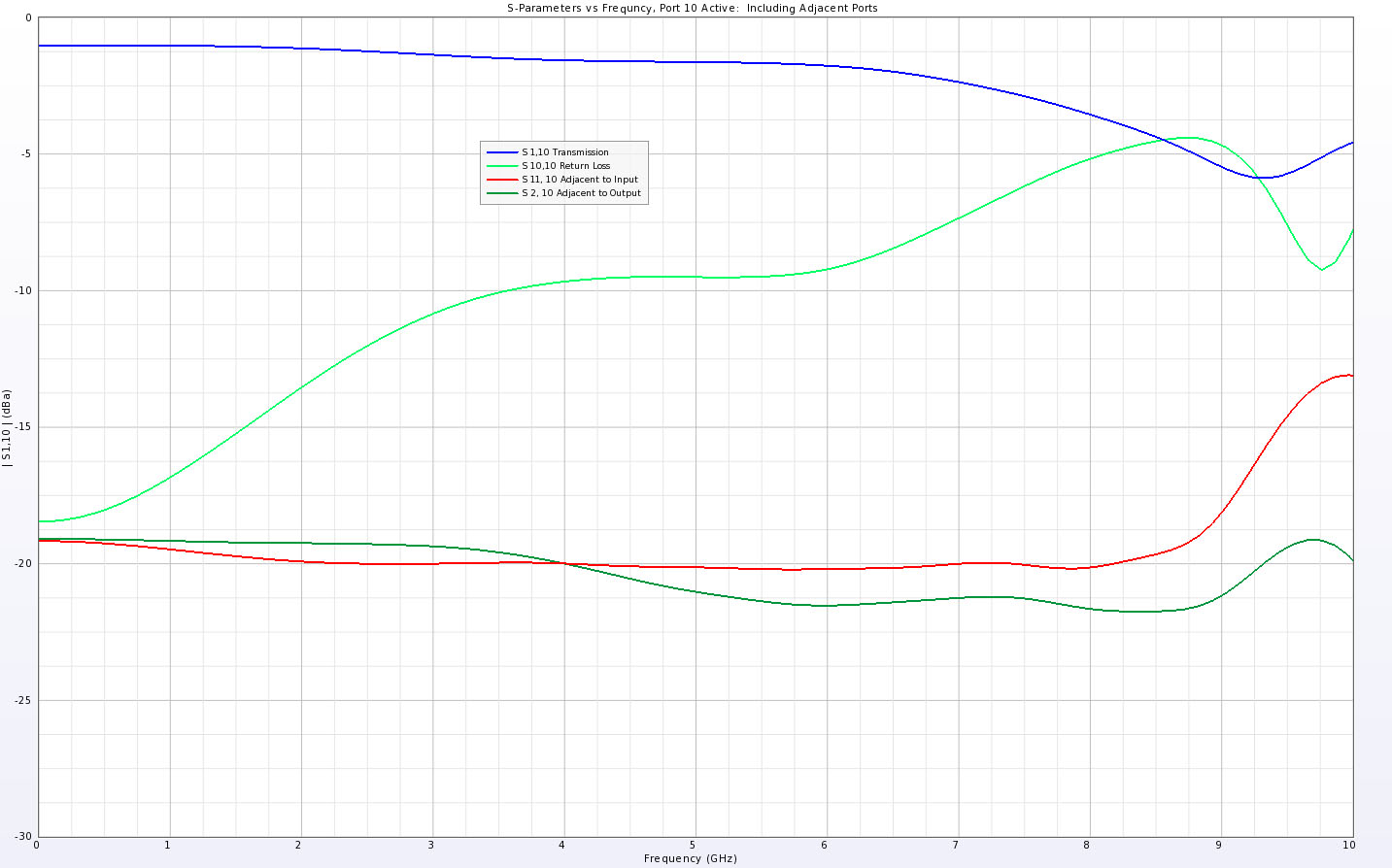
Figure 13: S-parameter results for the excited pin and ports adjacent to that pin.