Introduction
In this example, a circularly polarized dielectric resonator antenna is simulated in XFdtd to generate return loss, gain patterns, broadside gain versus frequency, and axial ratio. The antenna under study, which is intended for use as part of a compass navigation satellite system (CNSS) operating at bands of 1.268 and 1.561 GHz, has been taken from a journal paper [1] which includes both measured and simulated results. The results derived from XFdtd are comparable to those from the journal paper.
Device Design and Simulation
The antenna simulated here consists of a planar feed section and a large rectangular block of dielectric material with dielectric constant 20.5 centered over crossed slots in the ground plane. In Figure 1, a three-dimensional image of the simulated antenna is shown with the ground plane in red, the substrate in off-white, and the dielectric block in blue. The device is constructed on a 100mm x 100mm x 0.8mm substrate with dielectric constant 2.55. The feed structure consists of a microstrip line on the bottom of the substrate with a perpendicular stub for impedance matching. The ground plane above the substrate has two slots at 45-degree angles to each other, which are sized to produce modes for the dual-band circularly polarized behavior. A top view of the ground plane with the dielectric block removed is shown in Figure 2, while a bottom view of the microstrip line is shown in Figure 3. The microstrip line is fed by a distributed circuit component source at the edge of the substrate and with a waveform covering the frequency range of interest between 1 and 2 GHz.

Figure 1: A three-dimensional CAD view of the antenna geometry is shown with the dielectric resonator block visible at the center of the ground plane.

Figure 2: A top view of the antenna structure with the dielectric resonator block removed shows the crossed slots in the ground plane and the outline of the microstrip feed line on the bottom of the substrate.

Figure 3: The microstrip feed line with the impedance matching stub are shown on the bottom of the substrate.
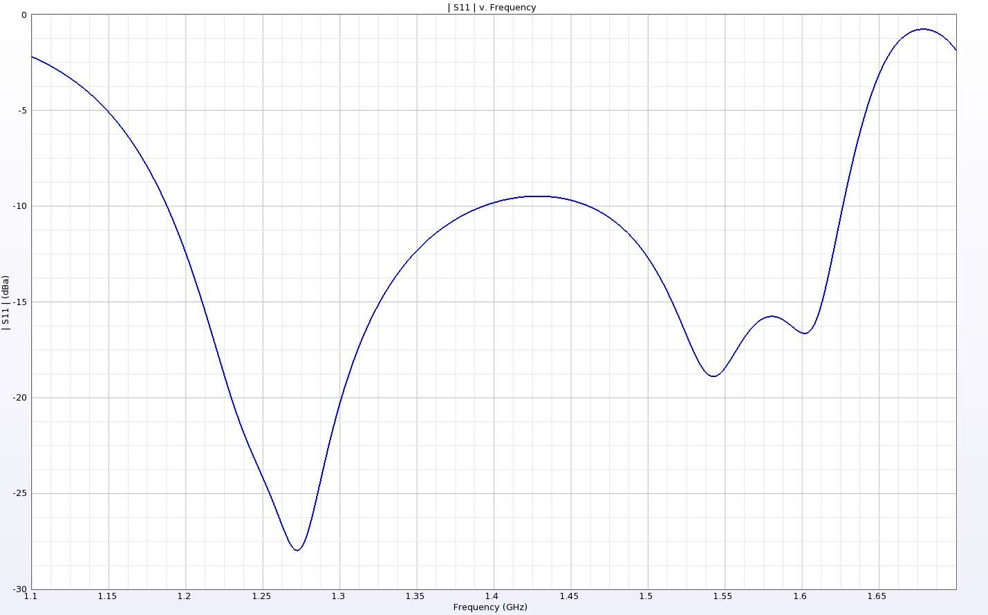
Figure 4: The return loss for the antenna shows two operating bands which correspond to the desired frequencies of 1.268 and 1.561 GHz
Following simulation, the return loss of the device is found to have two operating bands centered around 1.25 and 1.55 GHz (Figure 4). Each band is greater than 0.16 GHz in width and each is near the desired communication frequencies of the device of 1.268 and 1.561 GHz. Three-dimensional gain patterns at the two frequencies of interest are shown in Figure 5 and Figure 6 and indicate that the antenna produces nearly symmetrical broad lobed patterns with peak gain over 5 dBi directly above the dielectric block. The standalone radiation efficiency of the antenna is 100%, while the system efficiency is 81% and 66% at the two frequencies of interest. The peak gain value, which is at a point directly above the dielectric block, is plotted versus frequency in Figure 7 and can be seen to be quite consistent over nearly the entire frequency range of interest. Finally, the axial ratio, shown in Figure 8, shows a broad region of 3 dB bandwidth covering both bands of interest.
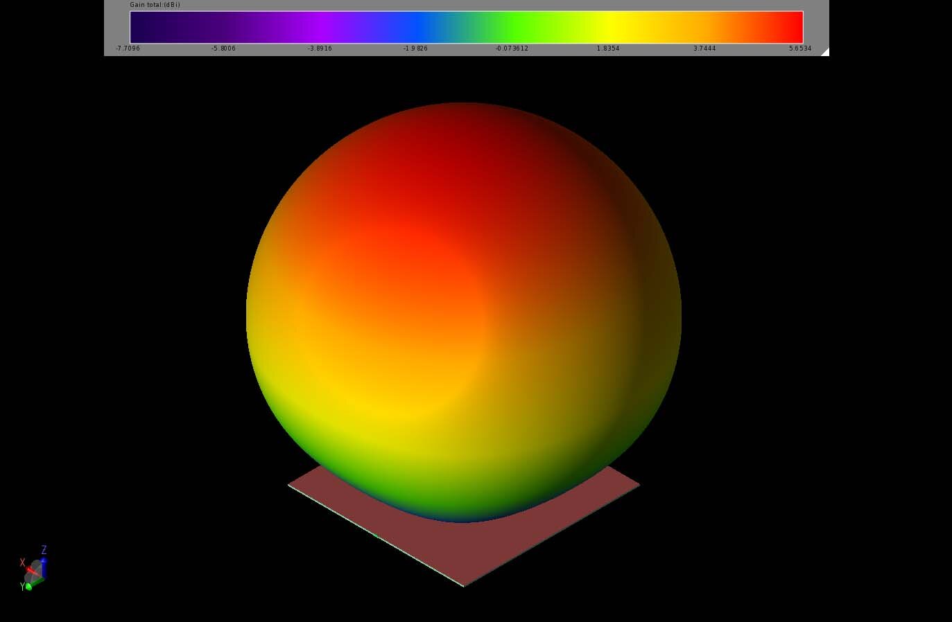
Figure 5: At 1.268 GHz, the gain pattern can be seen to be nearly spherical with a peak gain of 5.6 dBi above the dielectric block.
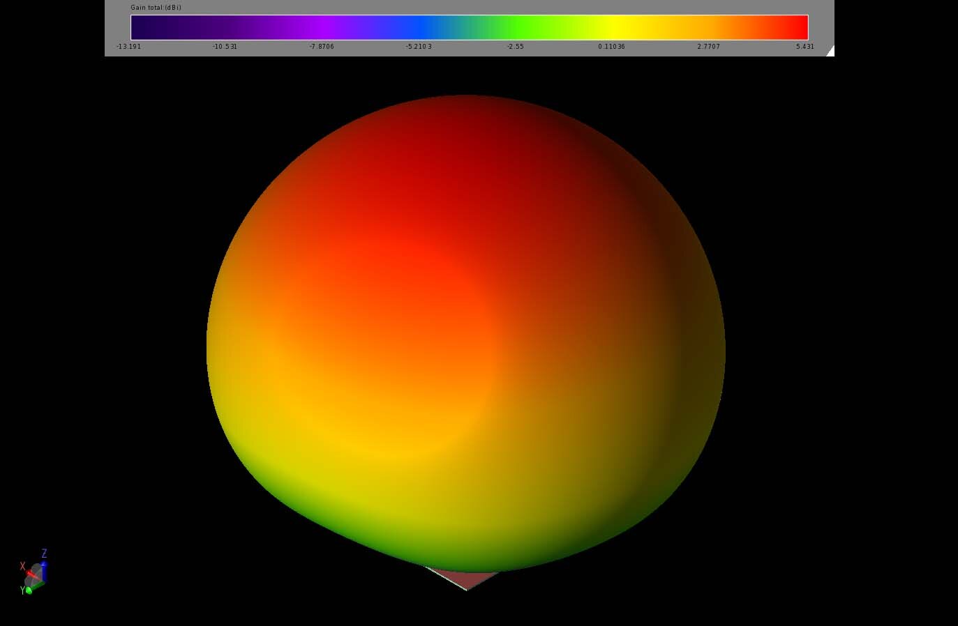
Figure 6: At 1.568 GHz, the gain pattern is nearly spherical and has a peak gain of 5.4 dBi in the direction directly above the dielectric block.
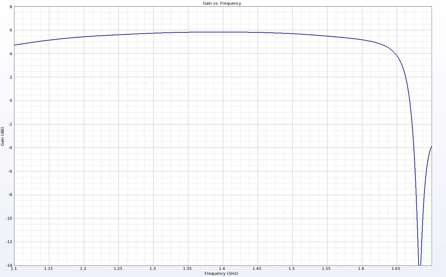
Figure 7: The gain at a point directly above the dielectric resonator is shown to be fairly consistent over a broad range.
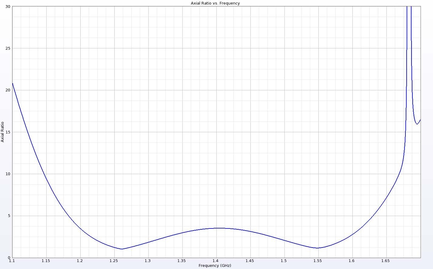
Figure 8: The axial ratio shows minima near the desired frequencies of 1.268 and 1.561 GHz and fairly broad 3 dB bandwidth.
Conclusion
Simulations of a dielectric resonator antenna are shown to produce good results, even with high dielectric constants of over 20. The return loss and gain patterns shown are good matches to the measured data shown in the referenced paper. The axial ratio of the simulated results shows better performance than the measured antenna, but the trends are quite similar and the results in the desired bands are good.
Reference:
X-C Wang, L. Sun, X-L Lu, S. Liang, and W-Z Lu, “Single-Feed Dual-Band Circularly Polarized Dielectric Resonator Antenna for CNSS Applications,” IEEE Trans. on Antennas and Propag., vol. 65, No. 8, pp. 4283-4287, Aug. 2017.