The crystal geometry is an array of rods, each 0.18125 microns on a side and spaced at a period of 0.58 microns with a curved waveguide line defect introduced by removing several rows of rods as shown in Figure 1. The dielectric properties of gallium arsenide are assigned to the rods. Also, in Figure 1, note the three red field sample points used to determine the frequency characteristics of this structure.
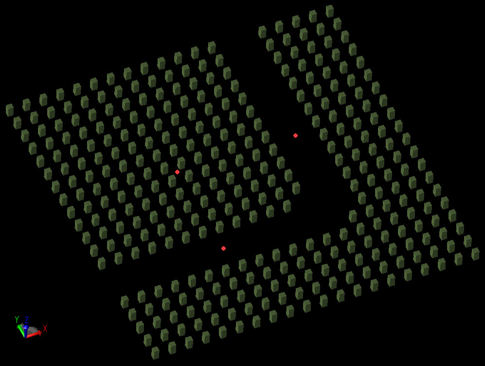
Figure 1: The two-dimensional array of rods.
Two simulations are run with this geometry. The first simulation determines the frequency characteristics using a broadband excitation. The second simulation shows the time domain progression of electric fields through the waveguide at a single frequency.
A waveform containing frequency content from 50 THz to 250 THz is applied to the structure at the center of the waveguide. Electric fields are collected at three points throughout the simulation. Figure 2 shows the normalized frequency response at each of the points and it can be seen that the waveguide supports frequencies between 150 THz and 200 THz.
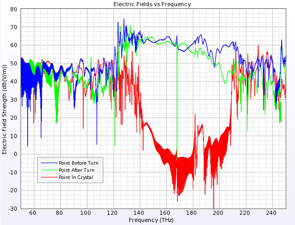
Figure 2: The supported frequencies in the waveguide.
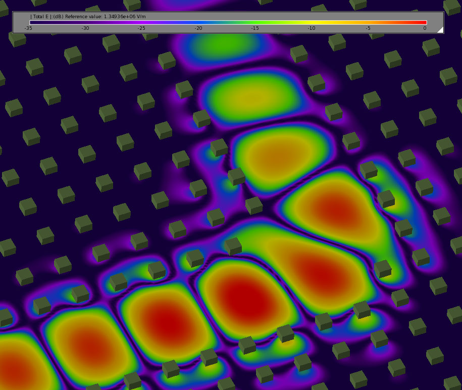
The broadband waveform was changed to a 160 THz sinusoid and time domain fields were collected as they traveled through the waveguide. Figures 3 - 5 show the propagation of the applied signal through the curve in the waveguide. The containment of the fields within the waveguide is clearly visible as the signal turns the corner and continues.
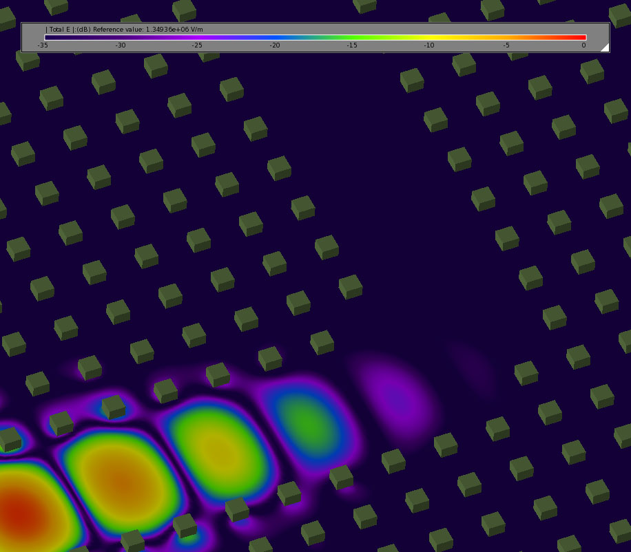
Figure 3: Time domain electric fields traveling through the waveguide at 160 THz.
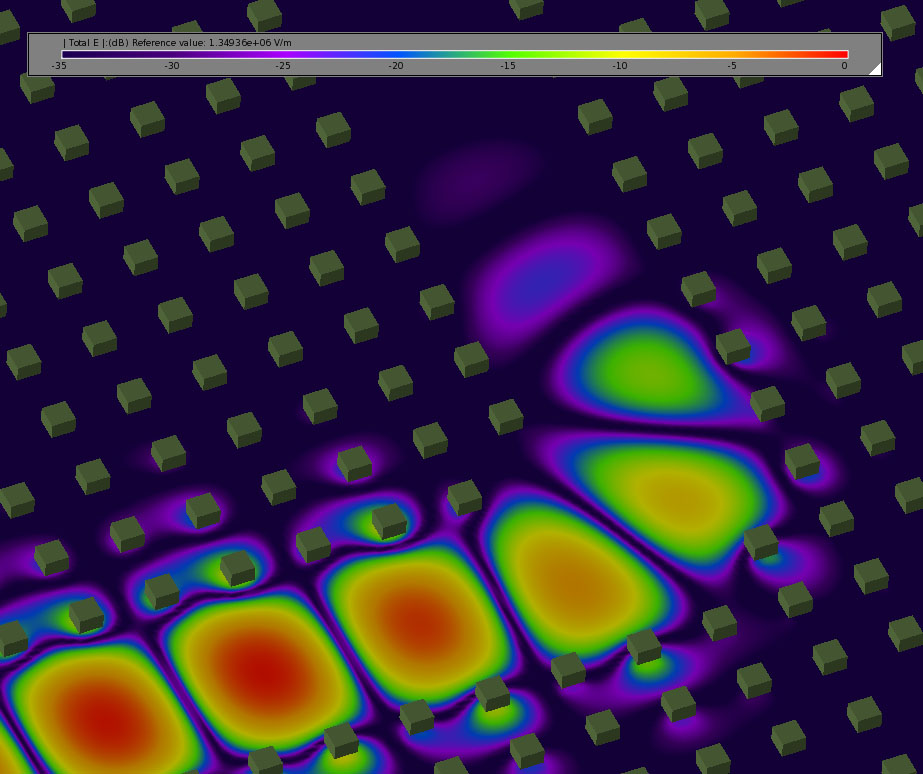
Figure 4: Fields are turning the corner.