This example investigates higher order modes available in waveguide ports in XFdtd. Here rectangular waveguides of WR187 size (47.55 x 22.15 mm) are used to create mode converters by introducing double or triple bends. The structures for this example come from a journal paper [1].
The first device considered is a dual bend mode converter shown in Figure 1. Here, two straight waveguide sections are connected to a center part that has two bends to form a partial "S" shape with the function of converting a TE10 mode to TE20 or vice versa. The device is constructed as a CAD model in XFdtd and then meshed in the software using the XACT Accurate Cell Technology conformal meshing feature to accurately describe the curvature of the waveguide. A cross-sectional view of the mesh is shown in Figure 2 where a base mesh size of 1 mm is used.
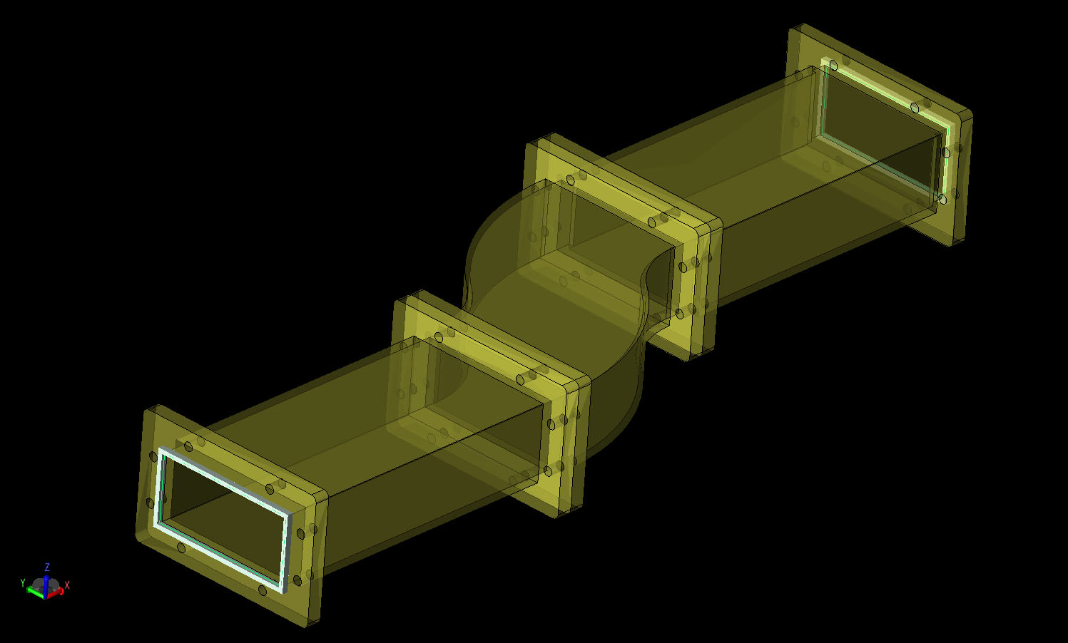
Figure 1: CAD geometry of the dual bend waveguide mode converter.
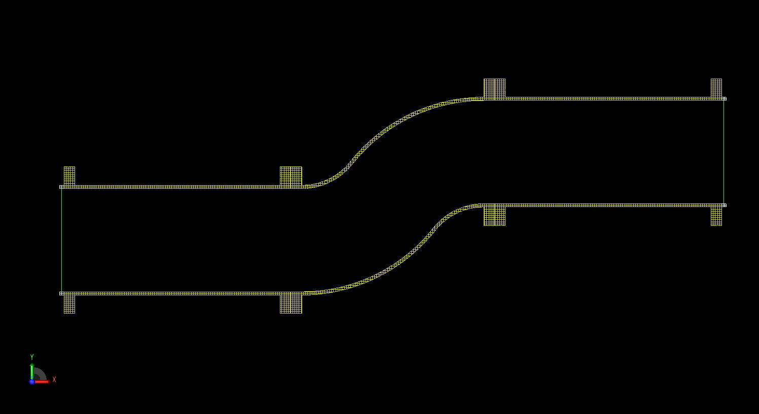
Figure 2: Cross sectional view of the XFdtd mesh of the dual bend geometry.
The simulation is performed with an input waveform with frequency content from 8-10 GHz with a TE10 mode active to create a TE20 mode at the output. The calculation is run on an NVIDIA Tesla C1060 GPU card and execution time is just over three minutes. Slightly more than 100 MB of memory are required.
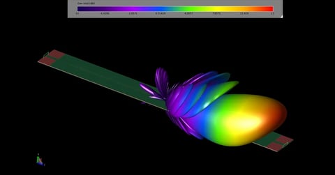
Following the simulation the steady state electric fields in the device are displayed at 8.5 GHz (Figure 3) to show the mode conversion that takes place in the double bend section of the waveguide. The steady state fields at the input and output ports are displayed in the angled view of Figure 4. The electric field in a line across the width of the output port is then plotted and compared to measured results from the paper [1] with very good agreement (Figure 5).
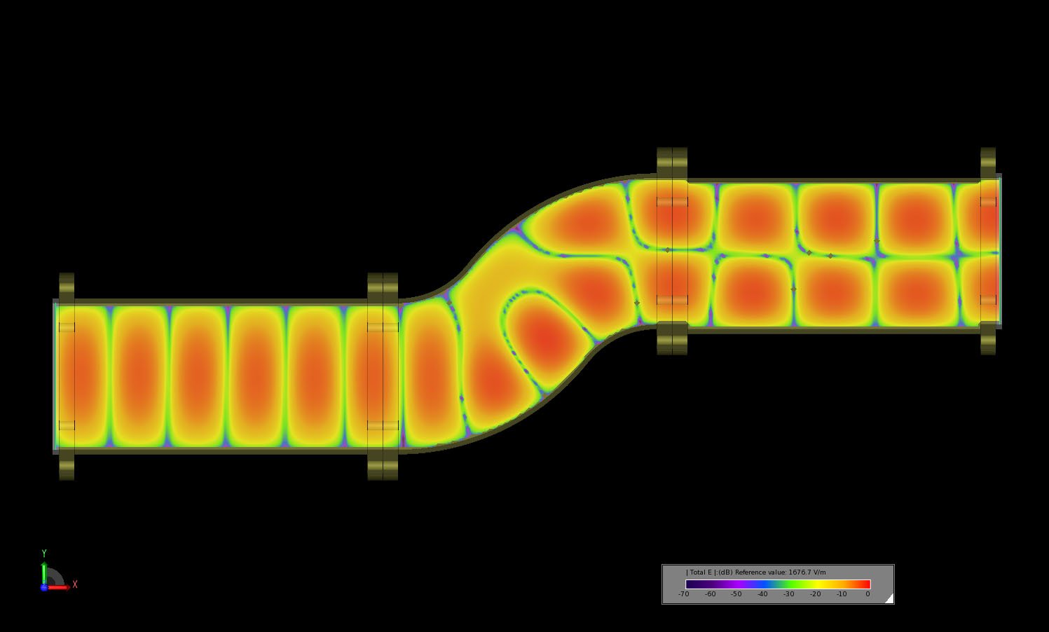
Figure 3: The steady-state electric field distribution in the dual bend converter at 8.5 GHz.
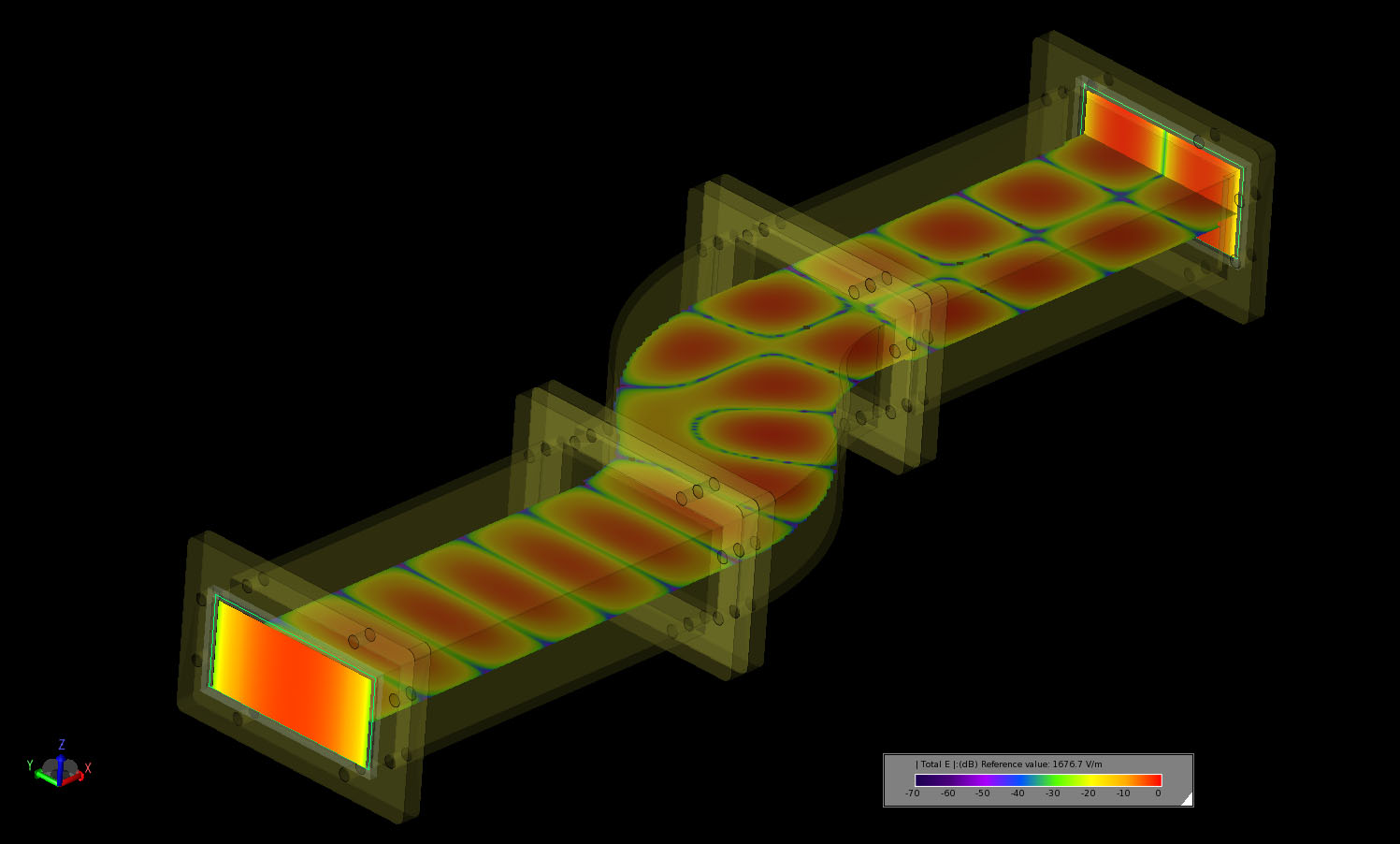
Figure 4: The steady-state electric field distribution in the dual bend converter at 8.5 GHz with the field distribution at each of the ports displayed.
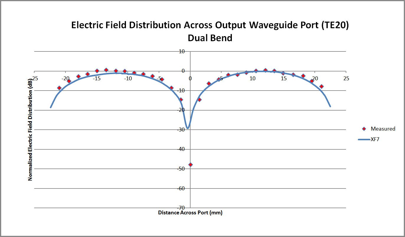
Figure 5: Comparison plot of the XFdtd electric field distribution across the dual bend converter waveguide port and measurements.
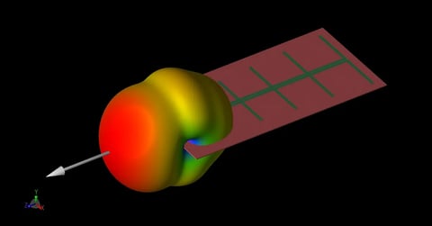
A second mode converter is created in a similar manner except in this case three bends are introduced into a section of waveguide, as shown in Figure 6. This device is meshed in the software with a 1 mm base cell size and the XACT feature. The resulting mesh is shown in a cross-sectional view in Figure 7. A TE10 mode is applied at the input port and the output TE20 mode is captured. The calculation is performed in just over two minutes in about 88 MB of memory. The resulting steady state electric fields at the port ends and through the center of the waveguide may be seen in Figure 8. The electric field across the output port is plotted versus measurements and again the agreement is very good as shown in Figure 9.
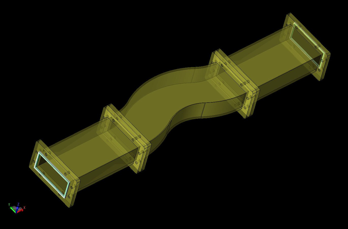
Figure 6: CAD geometry of the tri-bend waveguide mode converter.
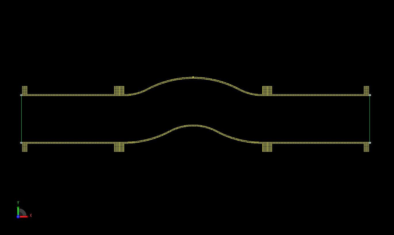
Figure 7: Cross sectional view of the XFdtd mesh of the tri-bend geometry.
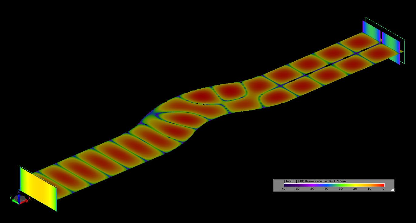
Figure 8: The steady-state electric field distribution at the ports and inside the tri-bend mode converter at 8.5 GHz.
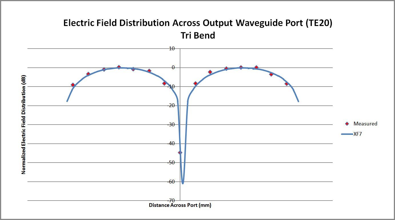
Figure 9: Comparison plot of the XFdtd electric field distribution across the tri-bend converter waveguide port and measurements.
As a final exercise, a combination of the previous mode converters is constructed to form a TE40 to TE10 device which is shown in Figures 10 and 11. The larger TE40 side connects to two tri-bend mode converters which are mirror imaged and produce an effect of putting the TE40 mode into TE20 form. An exponentially-tapered region is then added to reduce the waveguide size from two WR187 guides to a single WR187 which then feeds into a dual bend mode converter. The output of the dual bend converter is a TE10 mode.
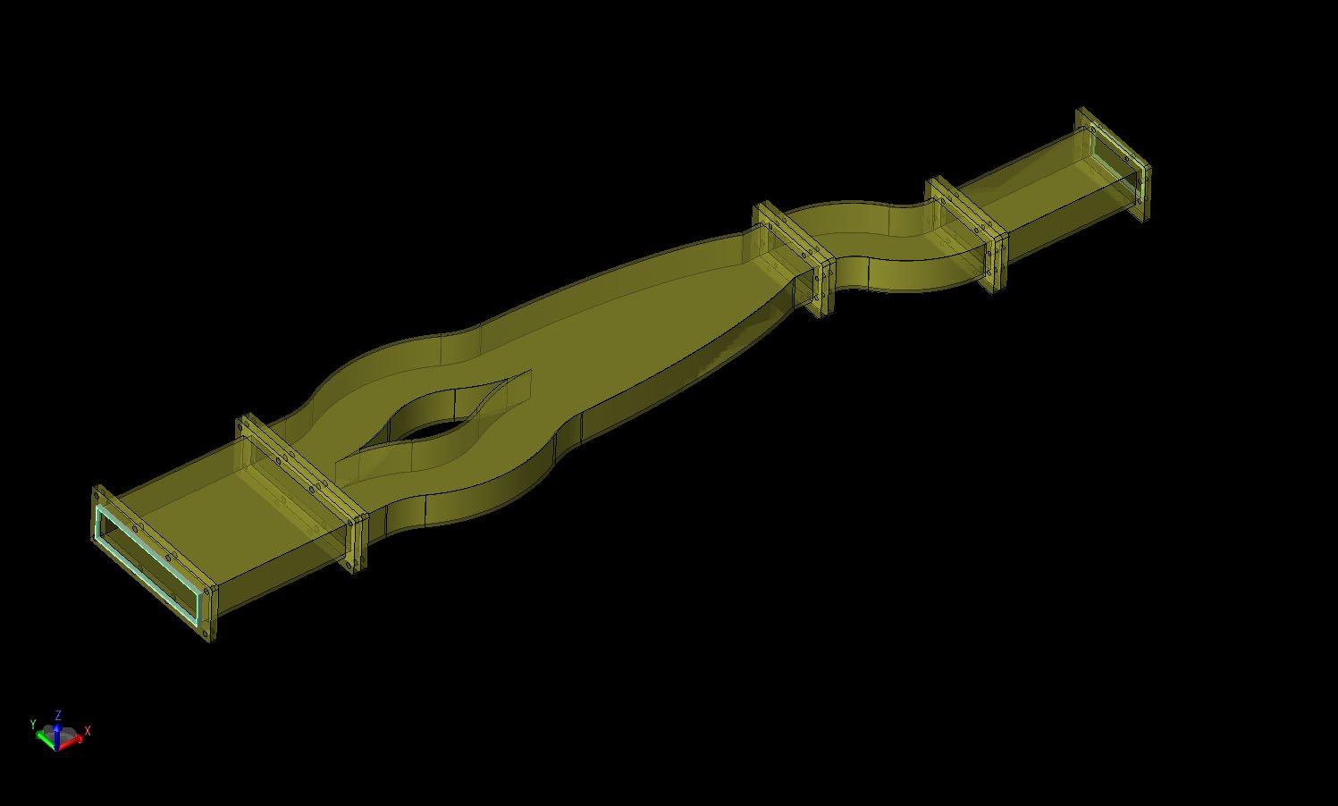
Figure 10: CAD geometry for the multi-mode converter shown in an angled view.
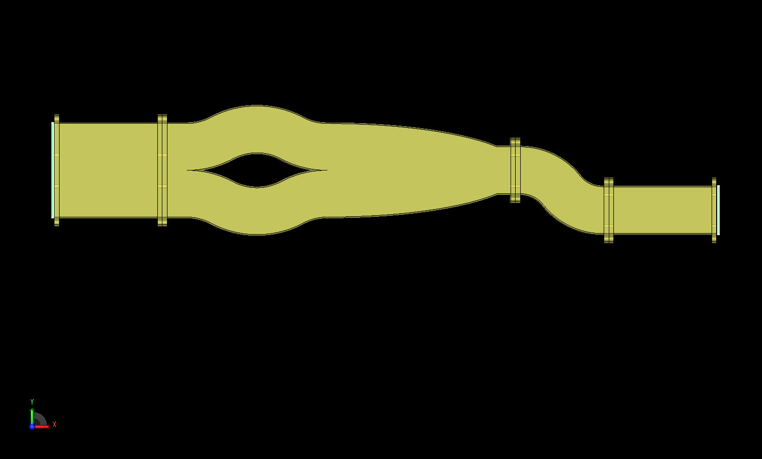
Figure 11: CAD geometry for the multi-mode converter shown in a cross-sectional view.
The simulation is performed with an 8.5 GHz sinusoidal input with the TE40 mode active and the output collected at the TE10 port. On an NVIDIA Tesla C1060 GPU card, the simulation converges to a -40dB level in approximately one and a half minutes using 274 MB of memory. The propagation of the TE40 mode into the output TE10 mode is shown in the transient field images of Figures 12 through 15 where each of the intermediate steps is also visible. The steady state electric field distribution in the waveguide and at the two ports is shown in Figure 16. The resulting electric field distribution across the output port is then shown in Figure 17.
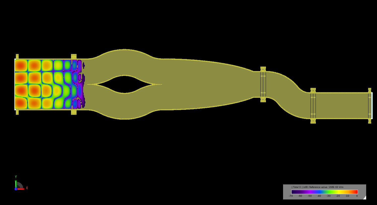
Figure 12: Transient electric field propagation in the multi-mode converter as the TE40 fields reach the entrance to the dual tri-bend converters.
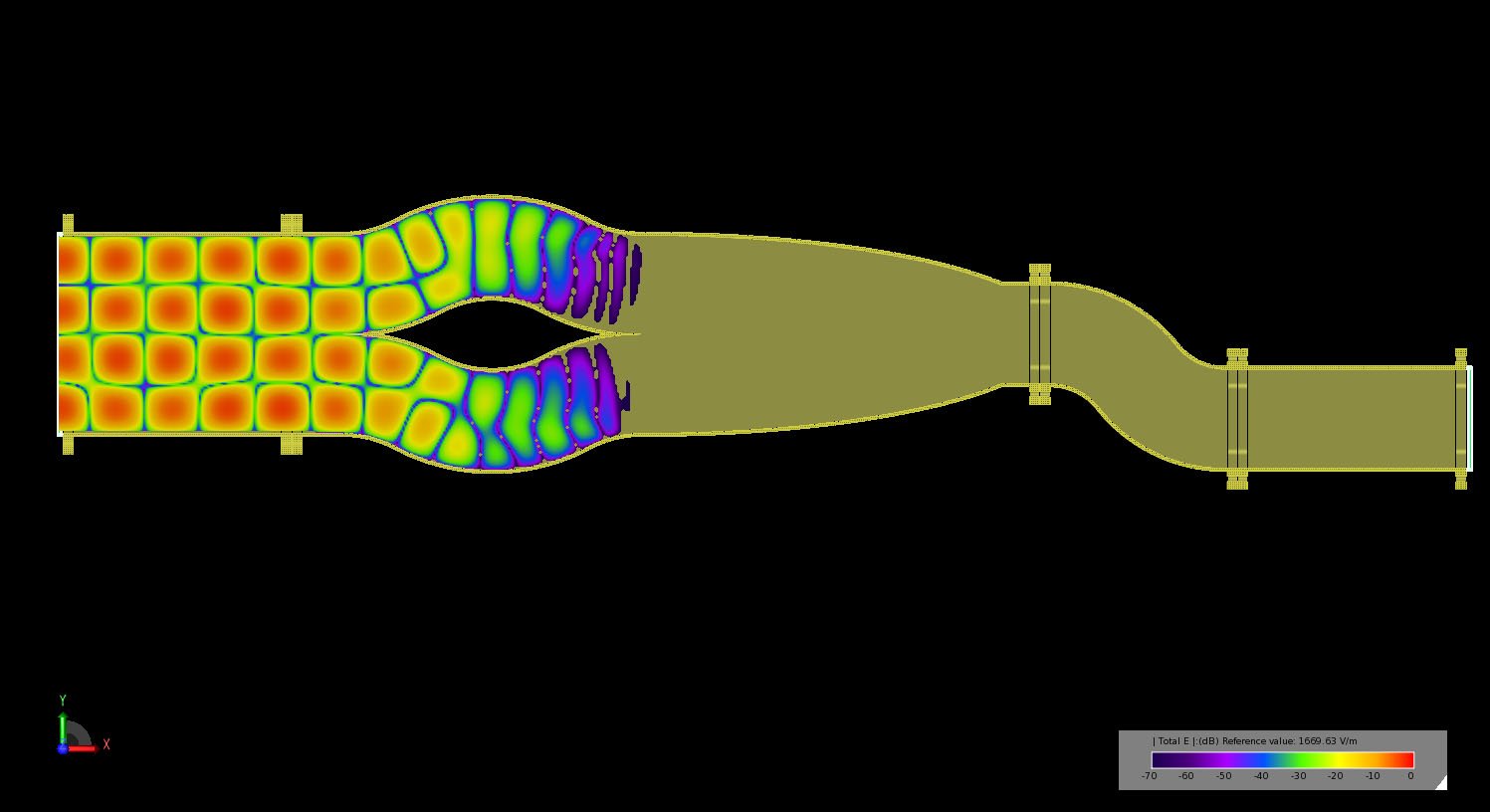
Figure 13: Transient electric field propagation in the multi-mode converter as the TE40 fields are converted to TE20 by the dual tri-bend converters.
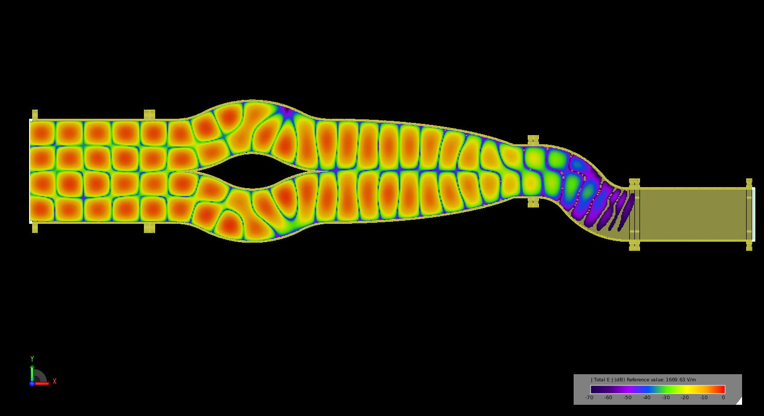
Figure 14: Transient electric field propagation in the multi-mode converter as the TE20 fields pass through the dual bend mode converter and are transformed to TE10.
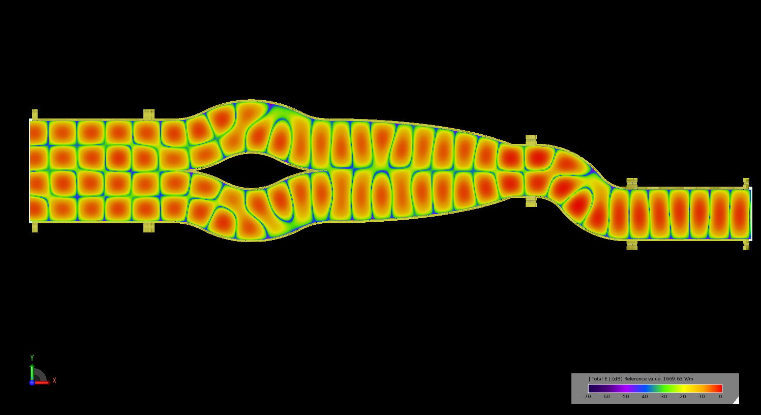
Figure 15: Transient electric field propagation in the multi-mode converter showing the complete path of the TE40 fields through the tri-bend and dual bend mode converters to the output port where they emerge as TE10.
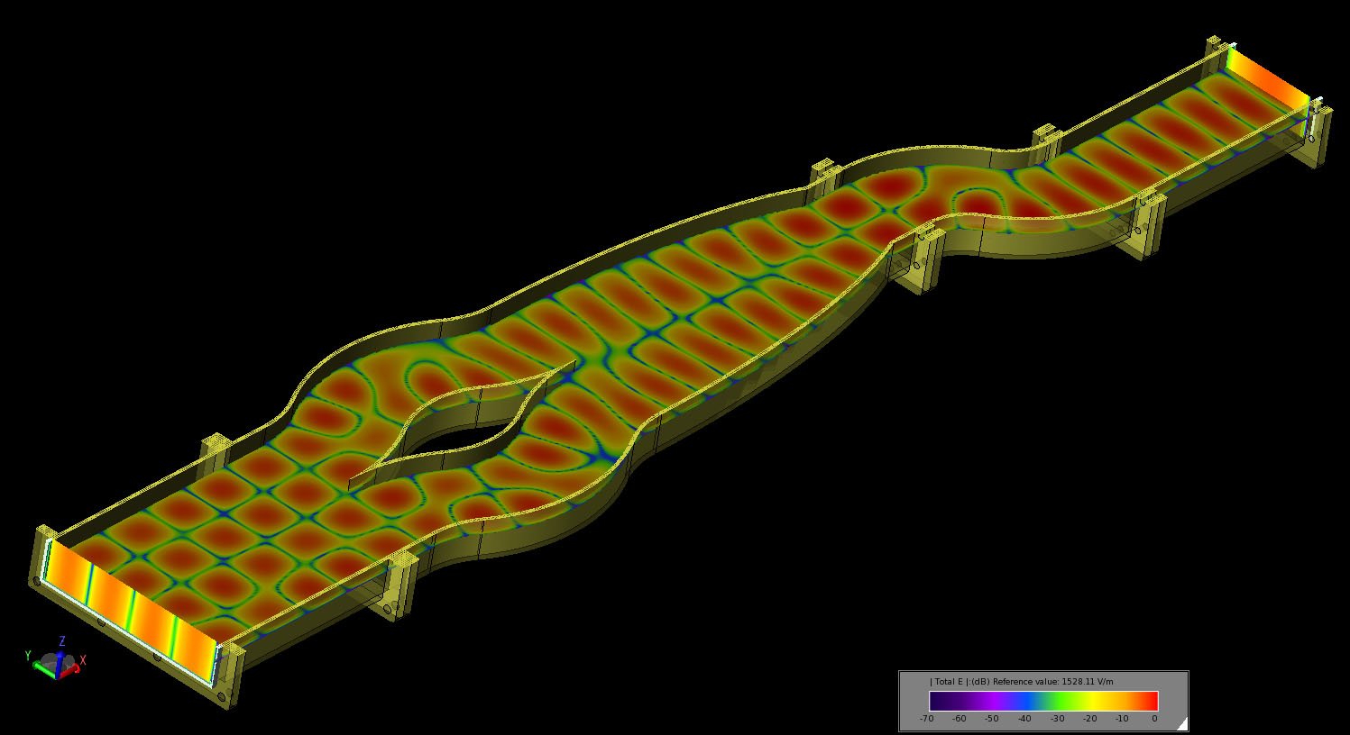
Figure 16: The steady-state electric field distribution at the ports and inside the multi-mode converter at 8.5 GHz.
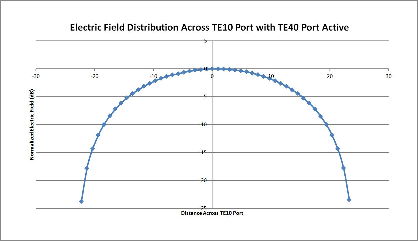
Figure 17: Plot of the XFdtd electric field distribution across the TE10 port of the multi-mode converter with the TE40 port active.
References
-
Q. Zhang, C. W. Yuan, and L. Liu, “Theoretical Design and Analysis for TE20-TE10 Rectangular Waveguide Mode Converters,” IEEE Trans. Microw. Theory Tech., Vol. 60 no. 4, Apr. 2012, pp. 1018-1026.