 Introduction
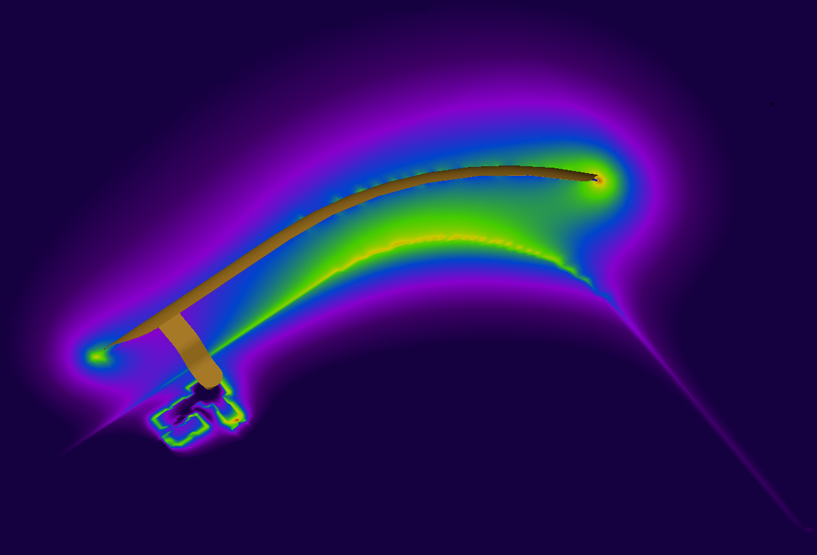
XFdtd 3D Electromagnetic Simulation Software analyzes antenna and matching circuit structures using the full wave Finite-Difference Time-Domain (FDTD) simulation method. XF’s Circuit Element Optimizer utilizes full wave analysis to select the component values for a given printed circuit board (PCB) layout. The selection process is guided by user-defined radiation efficiency or S-parameter goals and maintains accuracy by accounting for all EM phenomena affecting the matching circuit structure, such as coupling between antenna metal and nearby printed circuit board traces.
Circuit Component Simulation in FDTD
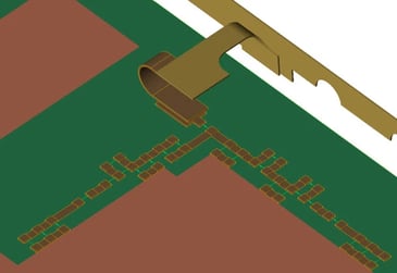
XF simulates ideal lumped circuit elements that are connected directly into the EM simulation mesh. The circuit elements get simulated in time-domain along with the EM simulation. In addition to discrete voltage source excitations and termination resistors, these circuit components can be antenna matching components including capacitors and inductors. These components are not partitioned out of the EM simulation into an ideal circuit schematic during simulation; they remain in place in the EM layout geometry. As a result, the circuit component simulation takes into account the signal trace losses, via inductance, ground return paths, and transmission line effects found by the full wave FDTD EM simulation.
Lumped circuit elements connected directly in FDTD mesh will be optimized.
Circuit Element Optimization
Building on XF’s ability to simulate lumped circuit elements connected directly to the EM mesh, XF’s Circuit Element Optimizer determines best component values based on the following goals:
-
Radiation efficiency
-
System efficiency
-
S-parameters
Using the full wave EM simulation with the matching circuit elements in place, XF characterizes the system and runs an optimization without moving the components into a different environment and adding ideal grounds. XF does not simulate the EM structure with each iteration of the optimization. Instead, the EM structure remains static, with all EM interactions taken into account, while the circuit components plugged into it are optimized.
The optimizer is able to determine optimal values for the following types of circuit components:
-
Fixed resistor, capacitor, inductor
-
Ideal resistor, capacitor, inductor
-
Realistic capacitor, inductor with user-defined equivalent series resistance
-
Passive tunable integrated circuits (PTIC or “tuners”)
Each component can take on a discrete range of values, representing the parts available from a component supplier.
Parasitics and EM Effects Are Taken Into Account
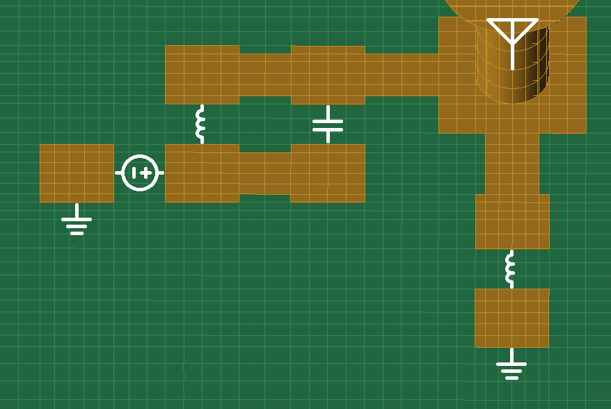
For high frequency and high performance circuit and antenna system design, EM simulation is utilized to see the complex and myriad electromagnetic coupling mechanisms, transmission line effects, and ground return current paths that affect and limit performance. By leaving the circuit elements in their final place in the circuit or antenna system layout, XF includes those EM effects on the circuit components even when they are being optimized. There is no need to move the circuit components into an idealized circuit schematic where these coupling and transmission line effects are lost. XF’s Circuit Element Optimizer uses all of the EM information available to arrive at the best possible optimized match. This capability is particularly popular in complicated, high performance applications such as mobile handsets, where XF optimization can even account for the effect of a mobile phone user’s head or hand on the antenna performance.
Full wave circuit optimization accounts for field coupling between antenna and matching network.
Design Workflow Using Circuit Element Optimization
The process typically starts with the design and EM simulation of an antenna structure. Once the complex impedance looking into the antenna is determined from EM simulation, a matching network topology can be chosen and candidate component values can be assigned. Next, the matching circuit is laid out in the design, including all of the details of interconnects, vias, and pads. This may be a PCB feeding the antenna or it may consist of circuit components attached to the antenna base or other nearby structure. After the matching structure and circuit element locations have been defined, the Circuit Element Optimizer is used to characterize the system and select optimal component values. Using user-defined goals and allowable values for each component, the Circuit Element Optimizer determines which component values best fit the goals. As validation, the chosen components can be plugged into a final full wave FDTD simulation or a physical prototype can be built and tested in the lab.