This example demonstrates the waveguide port source added with XFdtd in a complex structure of a cross-coupled filter [1]. The filter structure is comprised of a WR-90 waveguide that is folded in a tight curve with an aperture coupled-cavity at the bend of the curve. Several irises are inserted within the waveguide as well. Details of the design procedure are described in the paper.
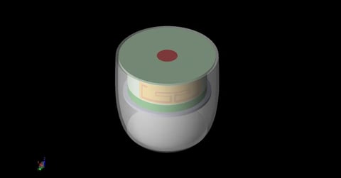
In the XFdtd simulation, the structure is first created as a CAD model as shown in Figure 1. The yellow portion of the structure is the waveguide filter while the two green rectangles at the edges represent the locations of the waveguide ports. The structure is created based on a parameter list for each dimension defined in the paper and shown in Figure 2. A global mesh size of 0.5 mm is used for this simulation with XACT Accurate Cell Technology meshing applied to the curved waveguide portion and Fixed Points meshing used for the waveguide ports. This configuration results in a varying mesh size which places grid lines precisely at the edges of each geometry feature. A cross-section of the resulting mesh is shown in Figure 3.
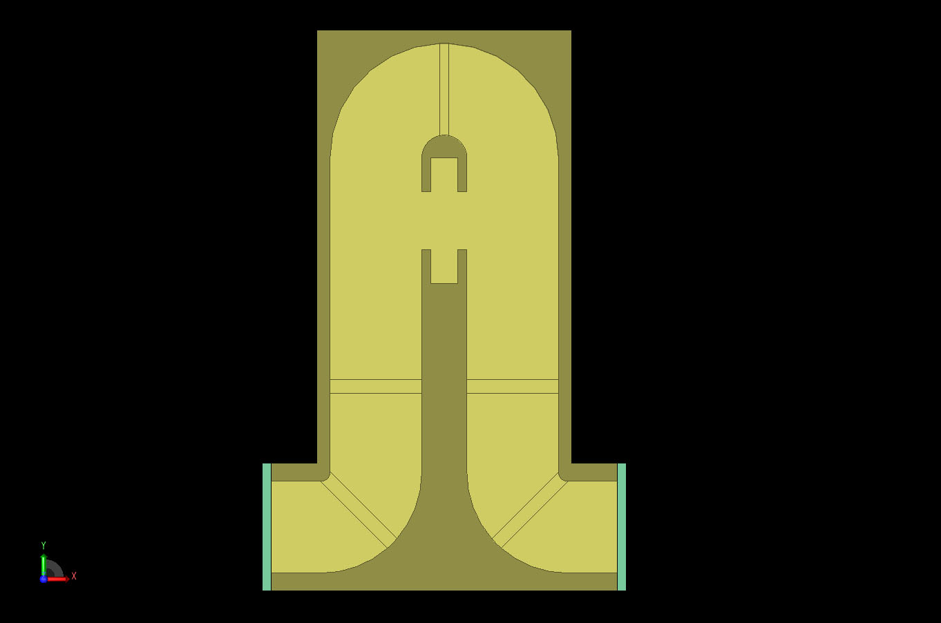
Figure 1: CAD representation of the waveguide cross-coupled filter geometry.
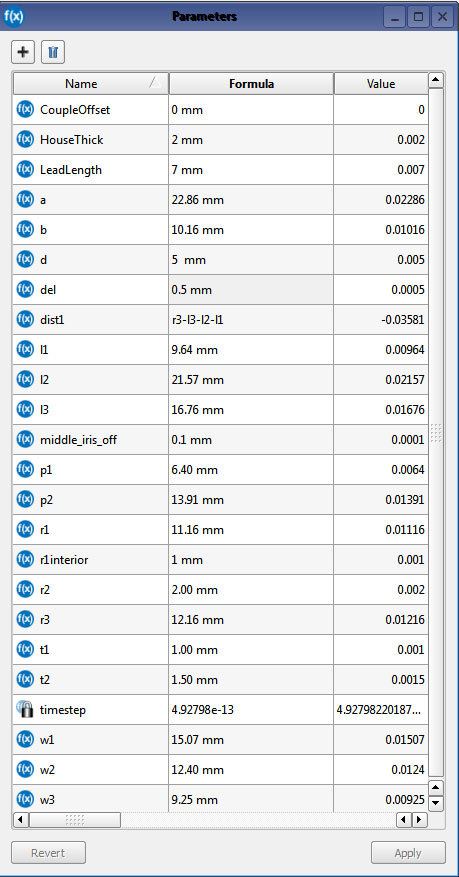
Figure 2: XFdtd parameter list of all dimensions used in the cross-coupled filter geometry.

Figure 3: Cross-sectional view of the XFdtd mesh of the cross-coupled filter geometry.
The ports are added across the openings of the waveguide and the distribution is set up as a TE10 mode, as shown in Figure 4 for the input port. The simulation is executed with an input waveform with frequency content over the 8-12 GHz range of the device. The time to complete the example to -45dB convergence is about 15 minutes on an NVIDIA C1060 Tesla GPU card. Following the simulation, the S-Parameters at the input and output ports are available and are displayed in Figure 5.
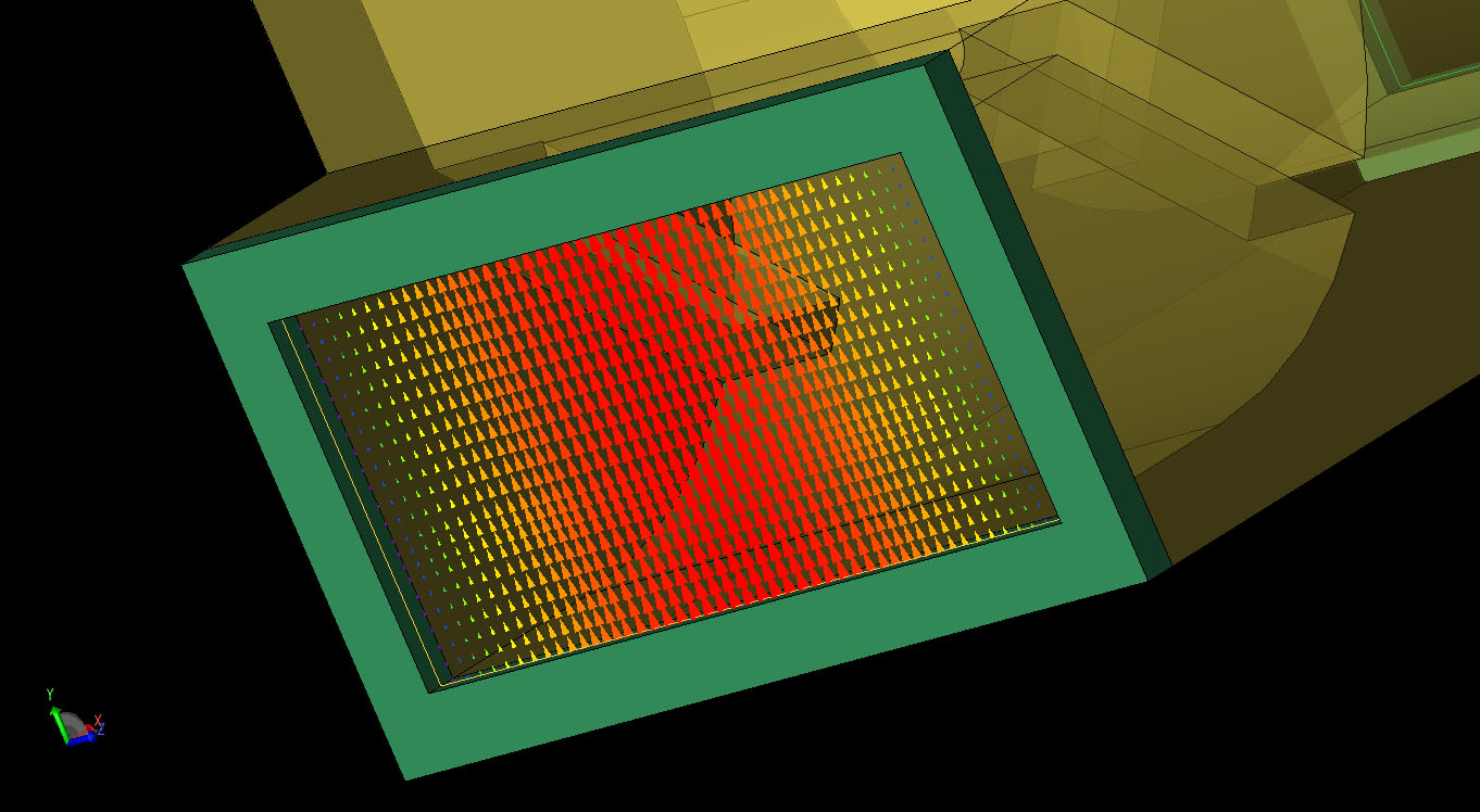
Figure 4: The TE10 waveguide port excitation applied to the input port of the device.
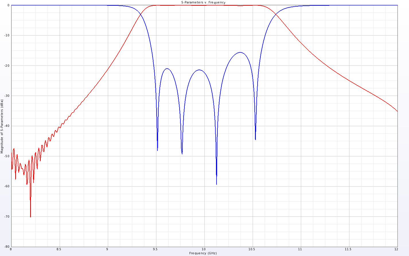
Figure 5: The computed S11 and S21 of the cross-coupled filter geometry.
References
-
Q. F. Zhang and Y. L. Lu, “Dimensional Synthesis of Symmetric Wideband Waveguide Cross-Coupled Filters Without Global Full-Wave Optimization,” IEEE Trans. Microw. Theory Tech., Vol. 58, Dec. 2010, pp. 3742-3748.