Introduction
This example describes a more developed 28 GHz antenna array capable of forming multiple beams for use in applications such as 5G network base stations. The system consists of three parts: a Rotman lens beamformer with seven input ports and eight output ports, a series of stripline Wilkinson power dividers to split each Rotman output into eight equal signals, and an 8x8 patch antenna array. The system will create seven focused beams with 3dB beamwidth of approximately 14.5 degrees and greater than 17 dBi gain that cover a +/- 30 degree area.
The design process consists of three separate stages: the creation of the Rotman lens beamformer, the design of the 1 to 8 Wilkinson power divider, and the 8x8 patch antenna array. The Rotman lens is designed as a microstrip device using Remcom’s Rotman Lens Designer® (RLD) software. The power divider and the patch array are designed in XFdtd®.
This example will describe the creation of each stage of the device and evaluate the performance of the individual stages and the full device.
Device Design
The Rotman lens beamformer is desired to operate at 28 GHz and to be able to scan seven beams +/- 30 degrees through eight array ports. A 50-ohm microstrip design is chosen which uses a circular contour shape and an overall width that is just under 5 wavelengths. The sidewalls are curved and include four dummy ports per side for absorbing any reflected fields. A suitable dielectric is chosen for the substrate with a relative permittivity of 2.94 and a thickness of 0.254 mm. The basic design is shown in Figure 1 where the RLD software used to create the lens is shown. The beam ports (input) are at the left of the image in grey while the array ports (output) are at the right in red. The output ports at the ends of the transmission lines are spaced a half-wavelength apart. The transmission lines are of varying lengths as determined by the equations of the Rotman lens. The Rotman lens is generally used with one or more beam ports active to produce a linear phase shift across the array ports due to the time delay in the signal propagation to reach the output. These devices are often referred to as “true time delay” systems and do not rely on phase shifters to steer beams.
Following tuning of the lens shape, the seven output beams, one per input port, are plotted in Figure 2 to verify the position of the beams and the sidelobe levels. The beams are present at +/-30, +/-20, +/-10 and 0 degrees of scan angle. A uniform aperture distribution array ports is intended.
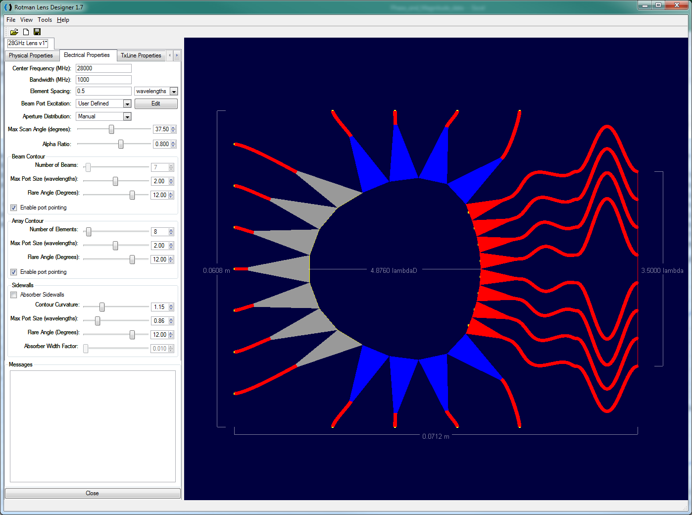
Figure 1: The initial Rotman lens design is shown in the RLD software. The seven beam ports are at the left and the eight array ports are at the right.
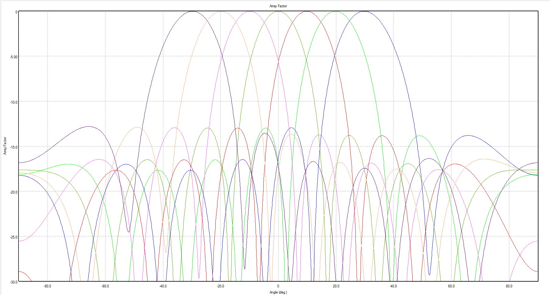
Figure 2: The Array Factor, a measure of the expected radiation pattern produced by a beam port due to the phase across the array ports, is shown for all seven beams of the Rotman lens designed in RLD.
Device Simulation
The Rotman lens design from RLD was exported into an SAT format CAD file for use in XFdtd. Following importation into XFdtd, the resulting geometry of Figure 3 was developed where all ports are terminated with a 50-ohm load. The return loss for each beam port was computed as shown in Figure 4 where acceptable values below -10 dB are found at 28 GHz. Via a script in XFdtd, the output complex voltages across the transmission lines connected to the array ports are used to compute the beam pattern for each input port which are shown in Figure 5. As can be seen, these are quite similar to the beams from the original RLD design.
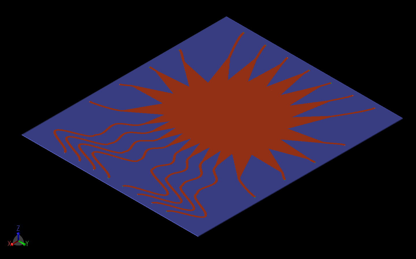
Figure 3: The Rotman lens design is shown in XFdtd following importation of a CAD file that was generated by the RLD software program. The lens is done in microstrip on a 0.254 mm substrate with permittivity of 2.94.
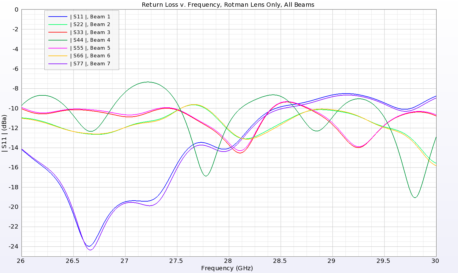
Figure 4: The return loss for each beam port of the Rotman lens is plotted over a frequency range around 28 GHz.
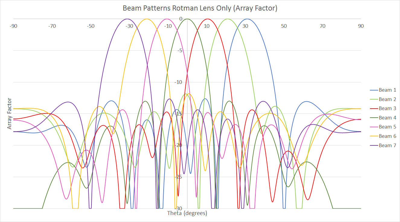
Figure 5: This figure shows the Array Factor for the Rotman lens as simulated by XFdtd. The complex voltage at the terminal end of each transmission line connected to the array ports was used to produce the Array Factor for each input port, and it can be seen that these beam patterns are very similar to those from RLD shown in Figure 2.
An analysis of the S-parameter data across the array ports shows that the magnitude has variations from -11 to -15 dB which are slightly more significant than the desired uniform distribution (Figure 6). The phase variations across the array ports show near linear variations, as desired, for each of the seven beams (Figure 7). In Figure 7 the phase is adjusted to put zero phase on array port 4 for comparison. The phase variation resulting from the Rotman lens between array ports is +/-90, +/-60, +/-30, and 0 degrees for the seven beams.
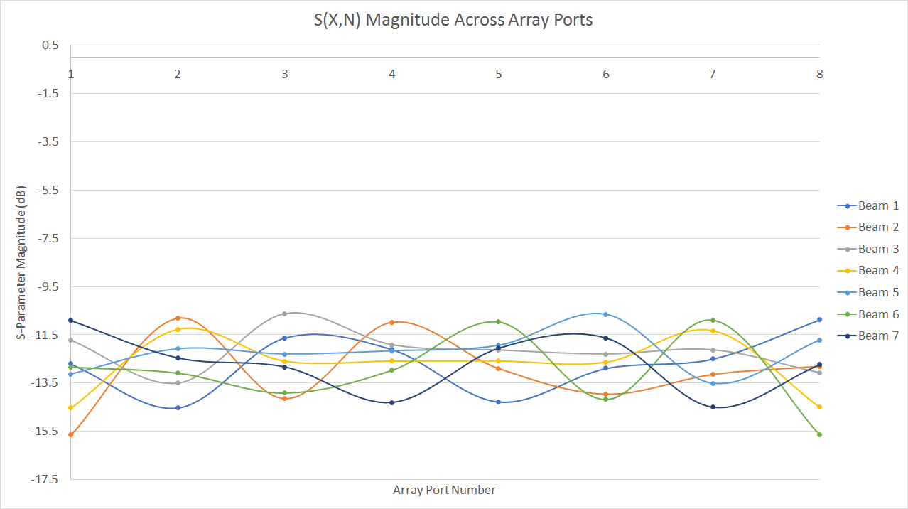
Figure 6: A uniform distribution across the array ports of the Rotman lens was desired in the design. In the XFdtd simulation, it can be seen that there is some variation in the actual distribution.
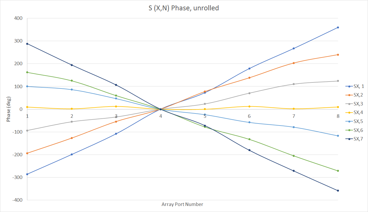
Figure 7: The phase variation across the array ports is plotted for each input beam port. The expected phase for the designed system should be linear with a slope ranging from +90 degrees between output ports to 0 degrees to -90 degrees depending on which input port is active. Here the phase variations can be seen to be nearly linear with slopes close to the desired values.
The stripline Wilkinson power divider is designed using the same dielectric (epsilon = 2.94) as for the Rotman lens. The thickness of the stripline substrate is 0.508 mm and the traces are 50 ohms. The design splits one input into eight equal and in-phase outputs in three stages. The output of each port of the Wilkinson is connected via a short coaxial cable to the input of a patch antenna. The patch antenna array consists of eight 1x8 subarrays where each subarray is connected to one Wilkinson. The patch array has a substrate of the same dielectric with 0.254 mm thickness. The patches are spaced a half-wavelength (at 28 GHz) apart and are tuned for best performance with a patch size slightly larger than a quarter wavelength and a feed offset by 0.9 mm from the center of the patch. The combined Wilkinson-Array parts are shown in Figures 8 and 9.
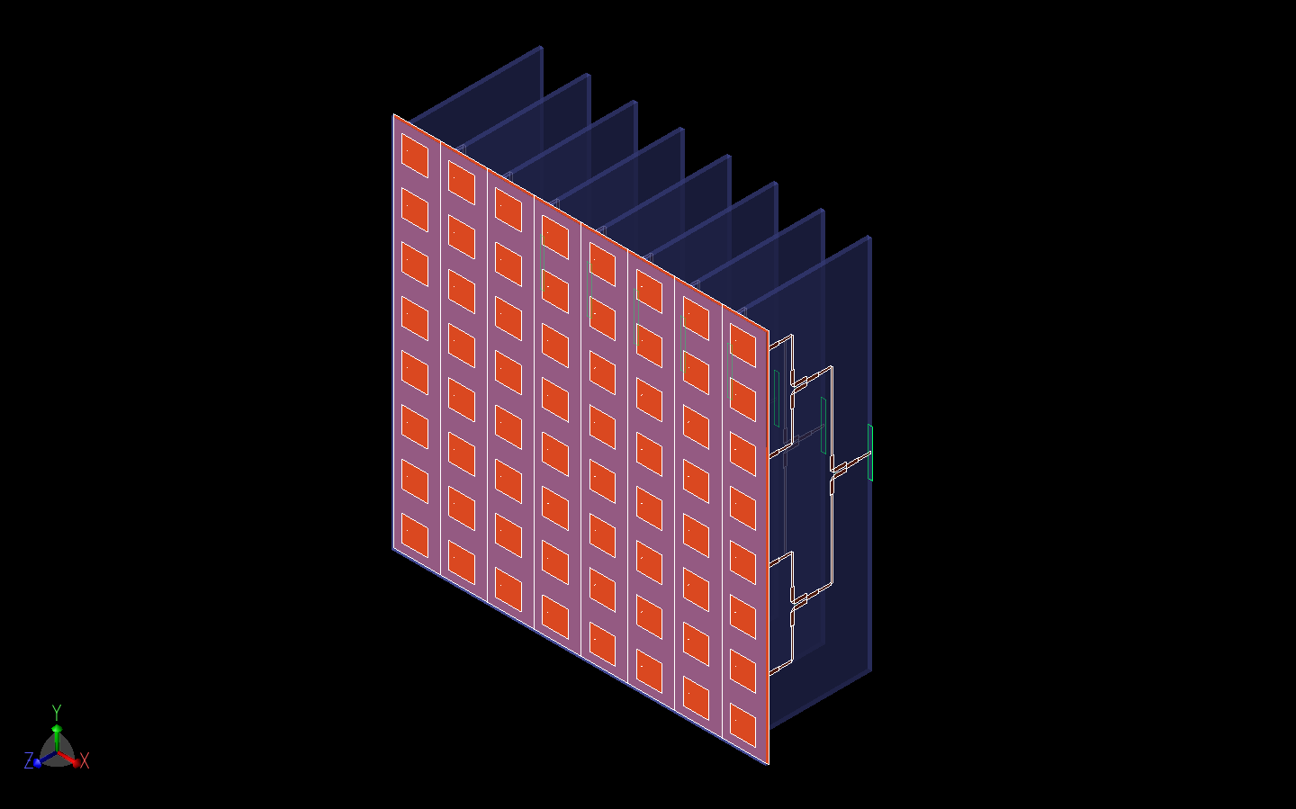
Figure 8: Shown in the figure is the three-dimensional CAD representation of the 8x8 patch antenna array and the eight Wilkinson power dividers that attach to the antennas. Here the Rotman lens has been replaced by eight input waveguide ports on the first stage of the Wilkinson power dividers.
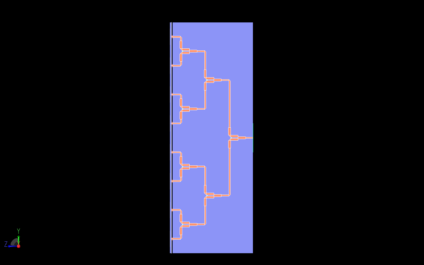
Figure 9: A side view of the Wilkinson power divider is shown which clearly displays the three stages of dividing the signal.
The combined Wilkinson-Array part was simulated with waveguide ports added to each of the eight Wilkinson inputs. The resulting return loss plots for each subarray are shown in Figure 10 and good performance is seen at 28 GHz. The ports are fed with phase shifts varying from +90 degrees between elements (beam 1) to -90 degrees between elements (beam 7) in 30 degree increments to produce seven distinct beams. The beam patterns (plotted as gain rather than Array Factor) are shown in Figure 11. In Figure 11 there is some slight variation in the peak gain, but the beam locations are well distributed at the desired angles which are a close match to the original RLD design. Figures 12 and 13 show the beams in three dimensions along side the geometry structure. The large white arrows indicate the direction of peak gain.
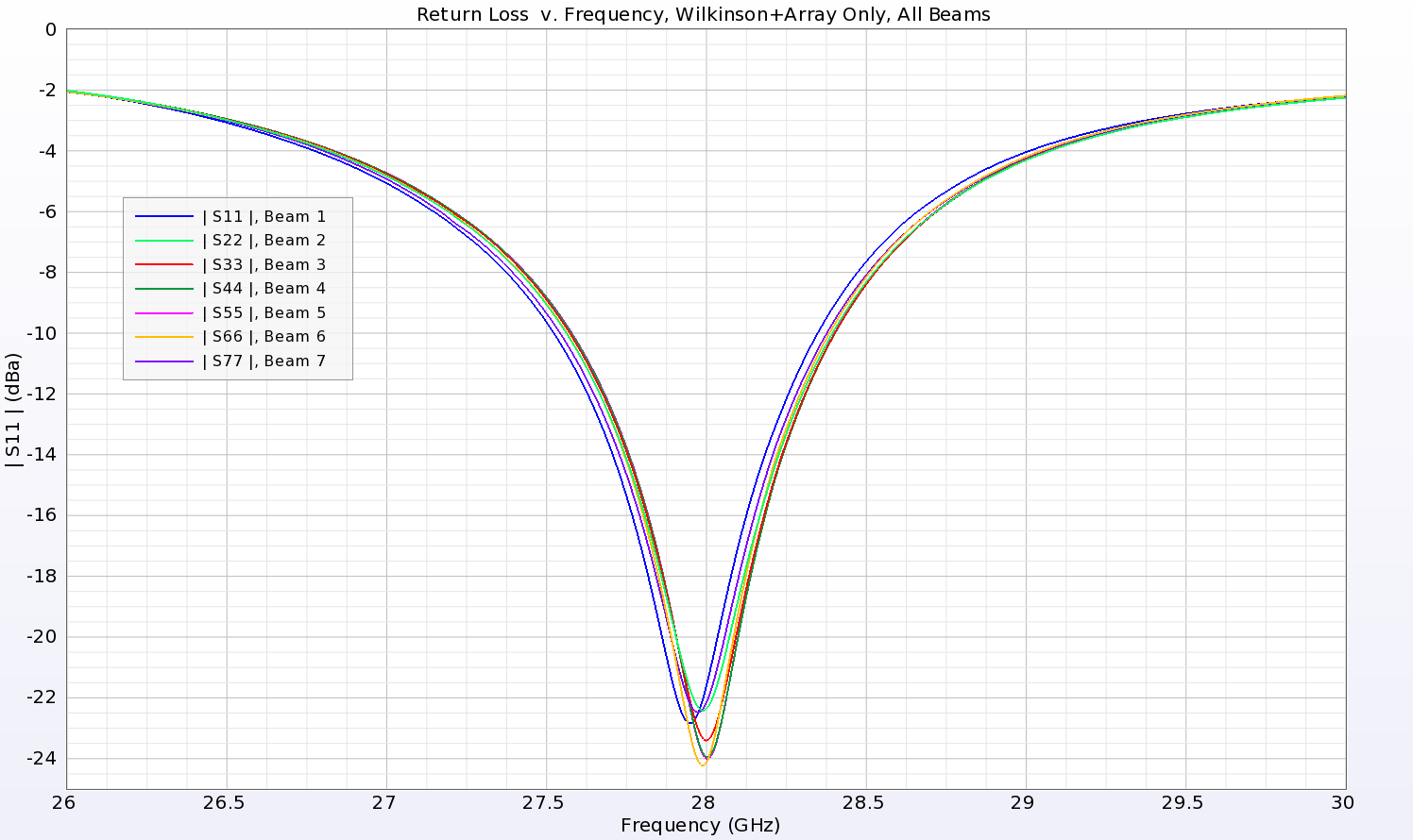
Figure 10: The return loss for each of the eight ports attached to the Wilkinson power dividers shows good performance at 28 GHz. There is only slight variation between the different 1x8 subarrays attached to each power divider.
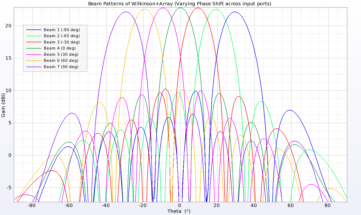
Figure 11: The beam patterns for the combined Wilkinson and antenna array are plotted as gain (rather than Array Factor) for the device of Figure 8. Here the phase relationships that would be produced by the Rotman lens have been replaced by phase shifts across the input ports attached to the Wilkinson power dividers. The beams can be seen to be in the correct angular position with nearly equal gain.
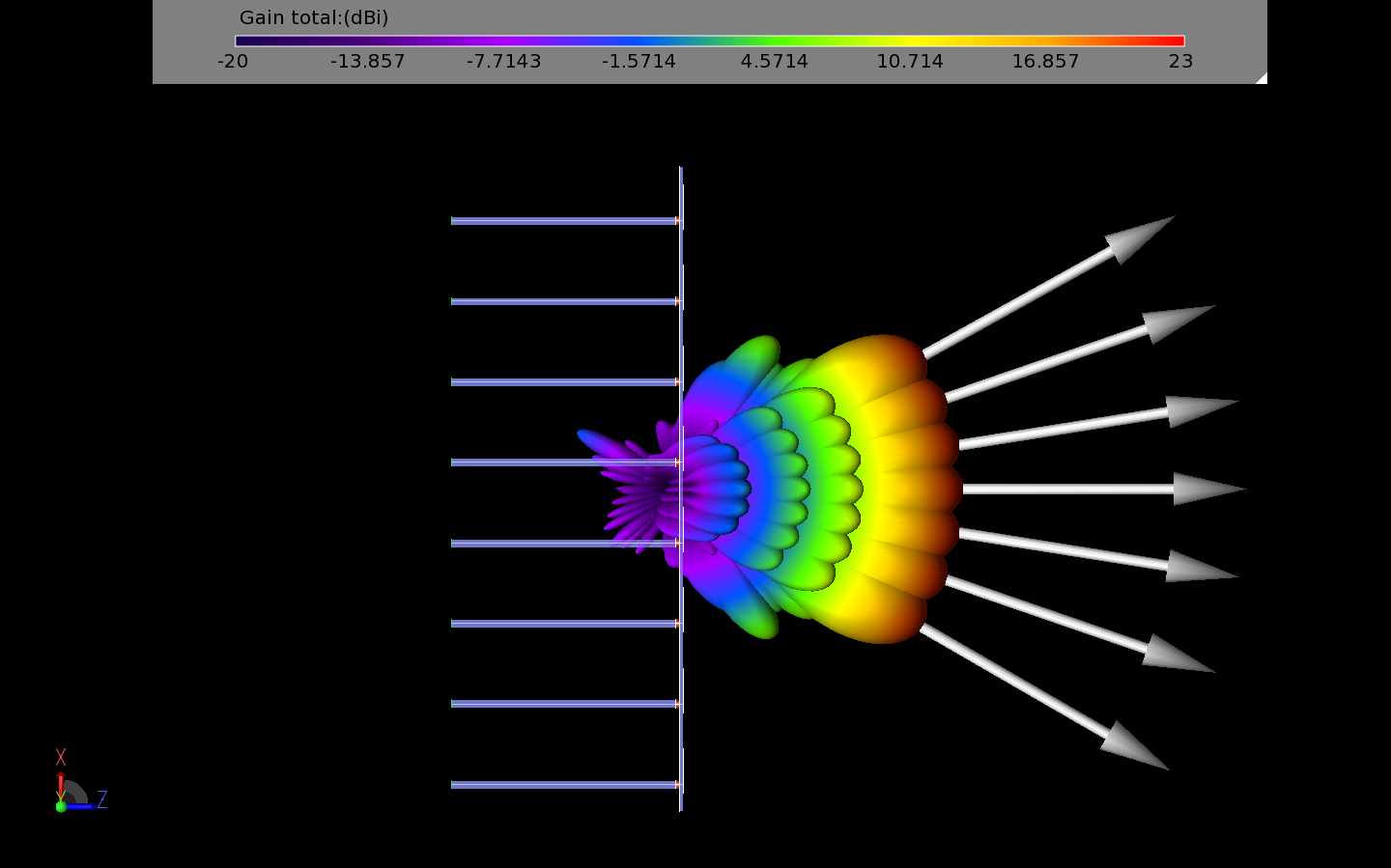
Figure 12: This figure shows the seven beams as a three-dimensional pattern rather than a line plot like Figure 11. The large white arrows depict the direction of the peak gain for each beam.
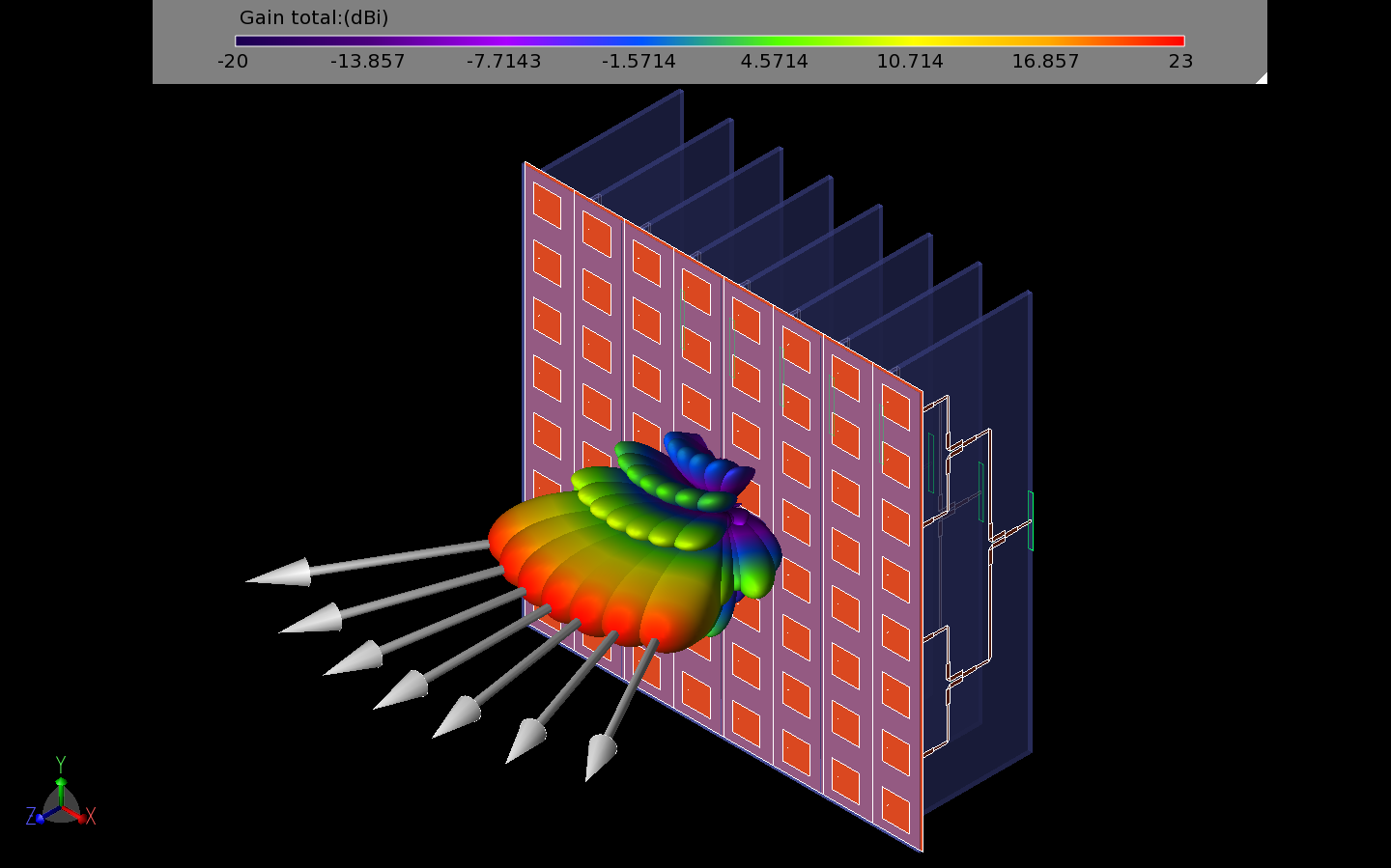
Figure 13: This is an alternate view of the three-dimensional beam patterns of the seven beams generated by the array.
The final step of the design is to combine the Rotman lens beamformer with the power divider/antenna array. This structure is shown as a three-dimensional CAD model in Figures 14, 15, and 16. Here, waveguide ports matched to 50 ohms are used at all open connections including the seven beam ports and eight dummy ports for reflection reduction in the lens.
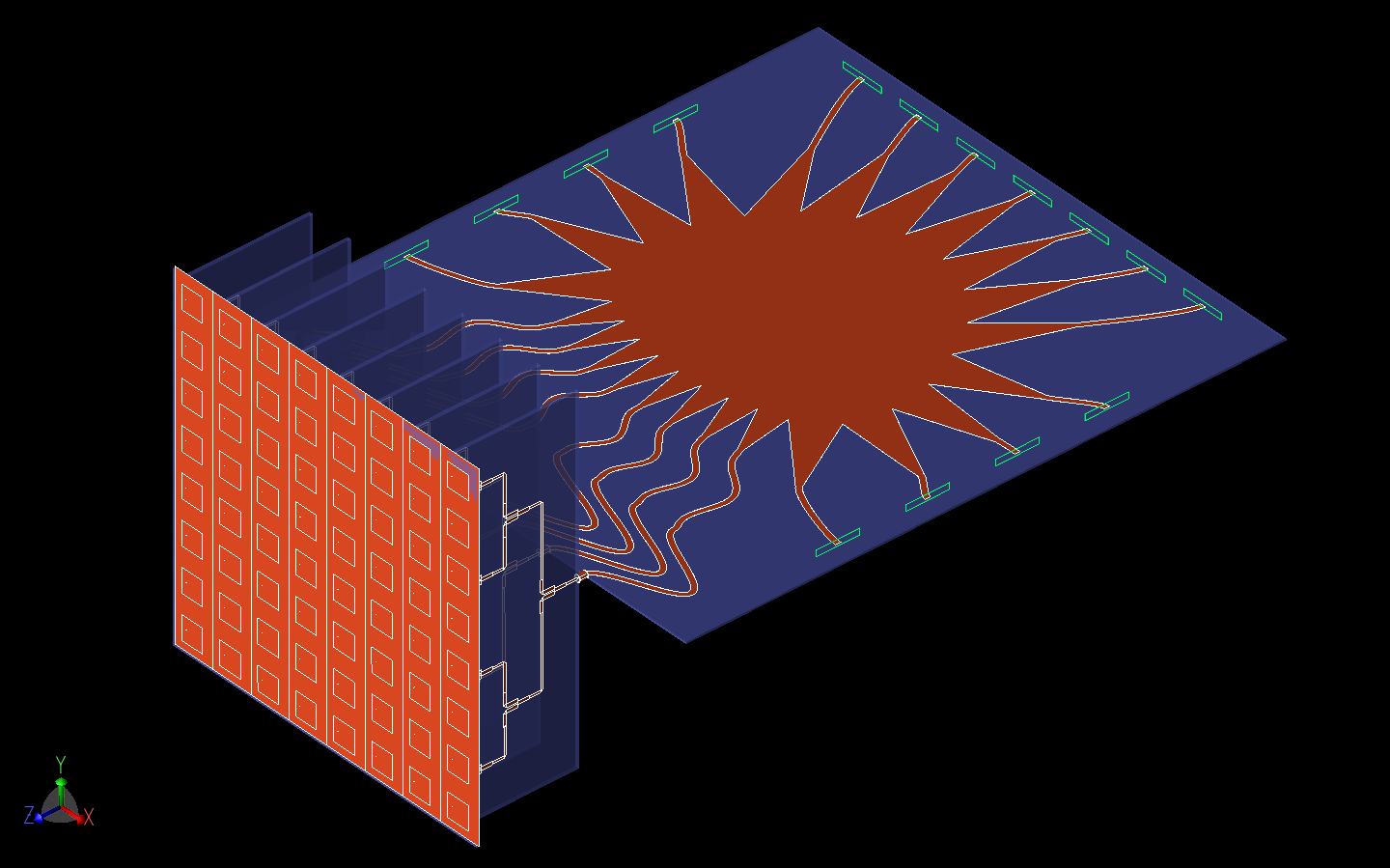
Figure 14: Here the complete system of the Rotman lens input, Wilkinson power divider stage, and 8x8 patch antenna array are shown as a three-dimensional CAD model.
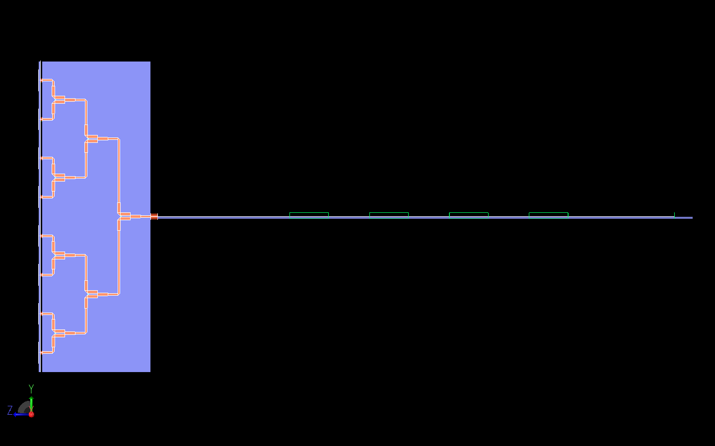
Figure 15: This is a side view of the entire system where the three stage Wilkinson power divider is more clearly visible.
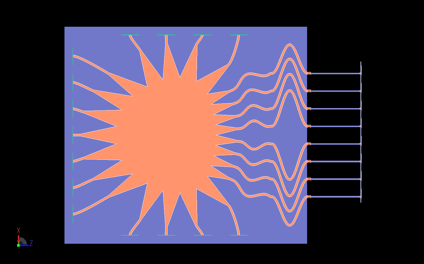
Figure 16: This is a top view of the entire system where the Rotman lens and array transmission lines are more clearly visible.
Following simulations with a broad band pulse at each beam port input, a plot of the return loss versus frequency is shown in Figure 17. The return loss for all ports is good and near -16 dB with the exception of the central port (beam 4) which has a higher return loss, perhaps due to the symmetrical location and reflections that are not well absorbed in the dummy ports.
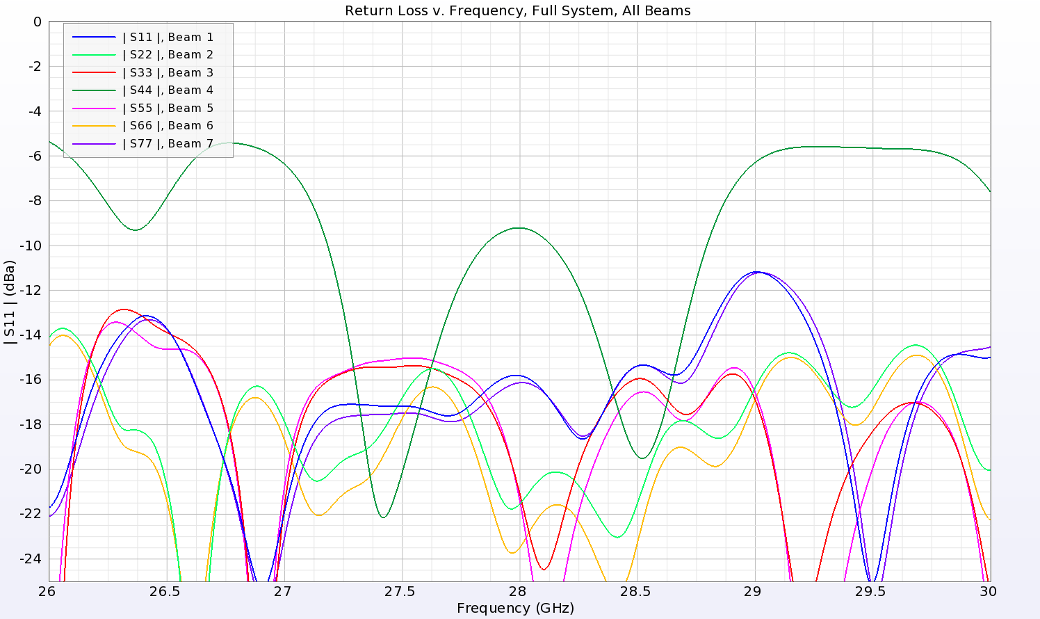
Figure 17: Plotted here is the return loss from each of the seven input ports of the Rotman lens when connected to the entire system of power dividers and antennas. The results are generally good with values below -10 dB for all ports except the center beam (port 4) which has some mismatch likely due to reflections not well absorbed by the sidewalls.
The beam patterns at 28 GHz for the full device are shown in Figure 18 and can be seen to be properly located in angle with somewhat higher variations in peak gain compared to the simulations of the array without the Rotman lens. This is due to the less-than-perfect phase and magnitude variations across the Rotman lens array ports that feed the Wilkinson power divider. The results are consistent with the previous beam patterns generated in earlier simulations shown in Figures 2, 5, and 11 despite showing more variation in the beam magnitudes.
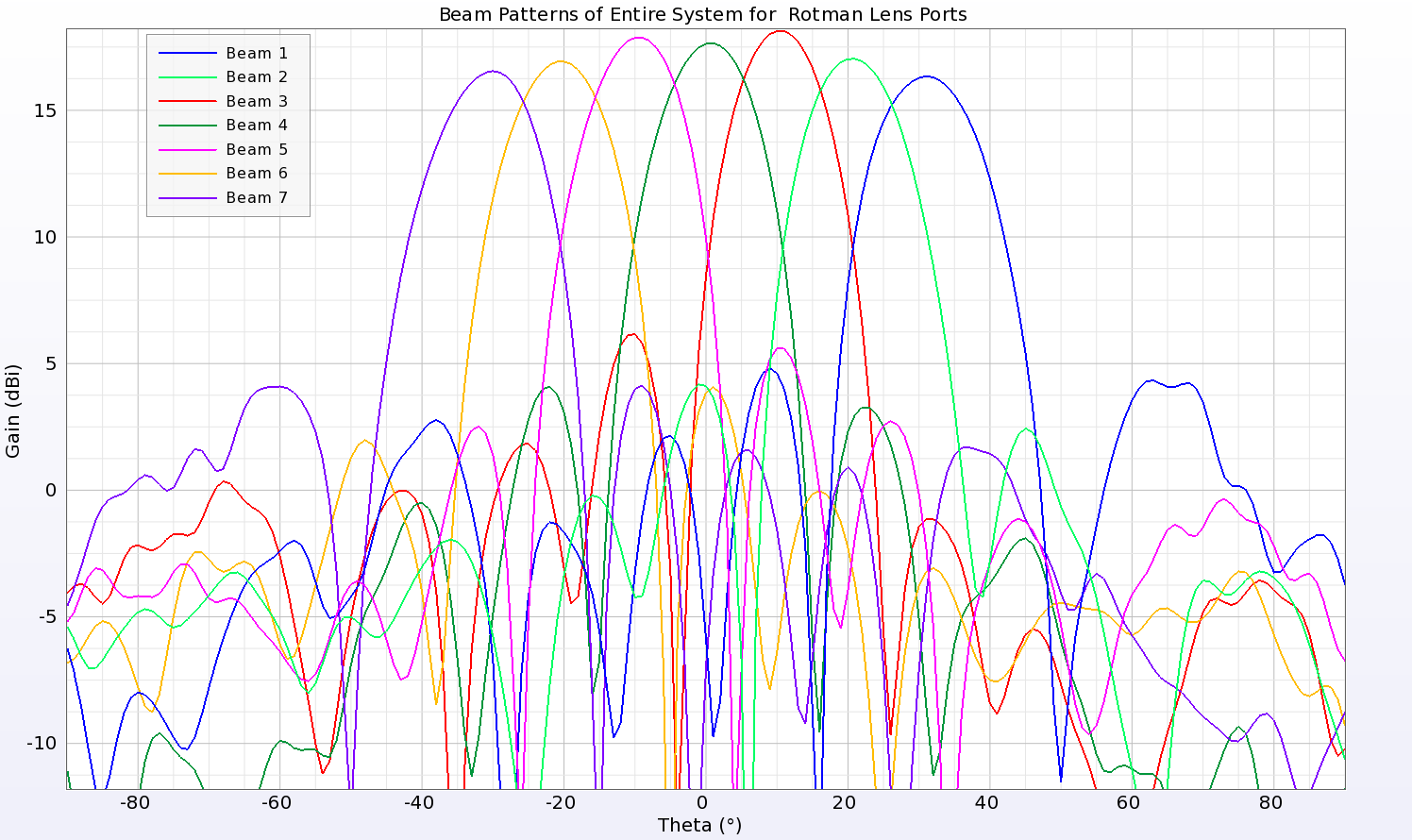
Figure 18: The resulting beams from the entire system are plotted as gain patterns and can be seen to be similar to the other beam pattern plots, with beams spaced 10 degrees apart from -30 to 30 degrees and near equal magnitude.
Three-dimensional views of the beams give a clearer image of the performance of the device including the presence of sidelobes and their levels. In Figures 19, 20, 21, and 22, the first four beams of the device are shown in relation to the device structure. Beams five, six and seven would be similar to three, two and one, respectively. In Figure 23, all seven beams are displayed in three dimensions to show the full range of coverage of the device. Figure 24 shows the same seven beams from a different viewing direction located above the device along the Y axis.
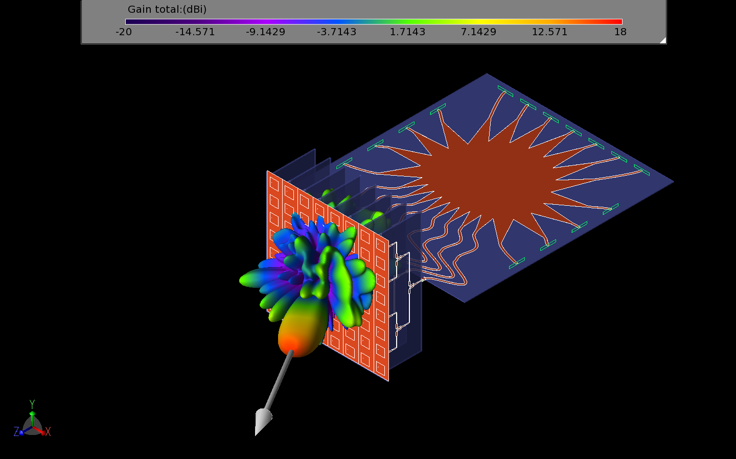
Figure 19: Shown in this figure is a three-dimension view of the beam pattern from input port 1 of the Rotman lens generated by the entire system.
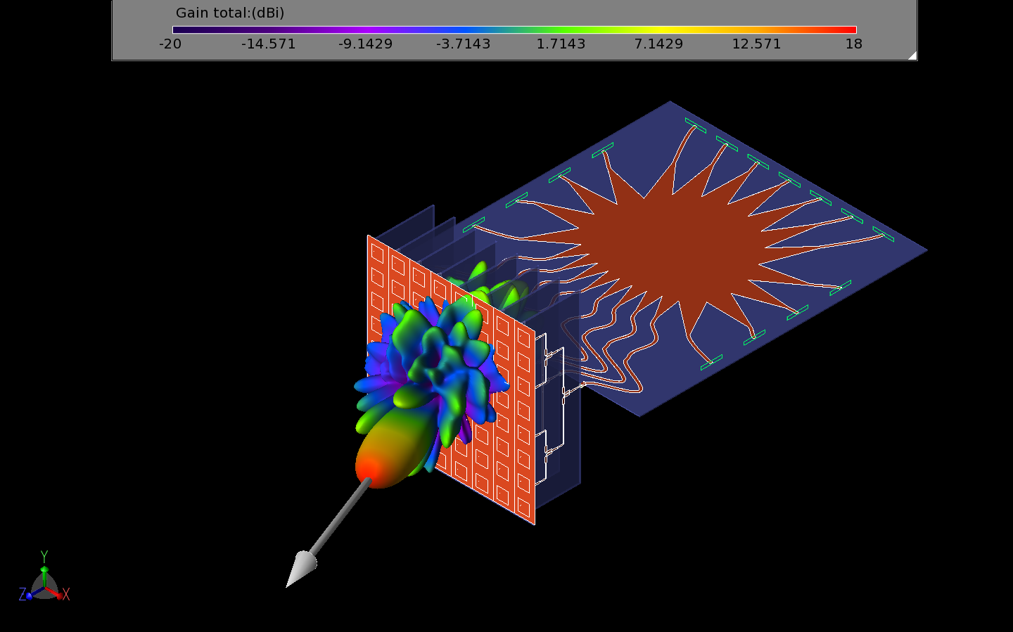
Figure 20: Shown in this figure is a three-dimension view of the beam pattern from input port 2 of the Rotman lens generated by the entire system.
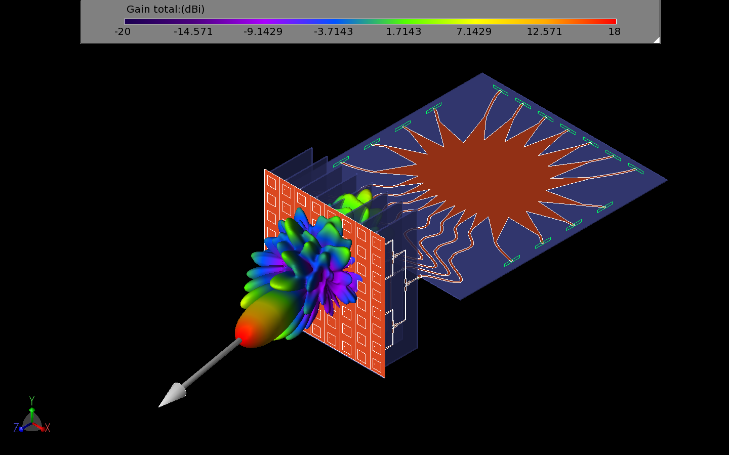
Figure 21: Shown in this figure is a three-dimension view of the beam pattern from input port 3 of the Rotman lens generated by the entire system.
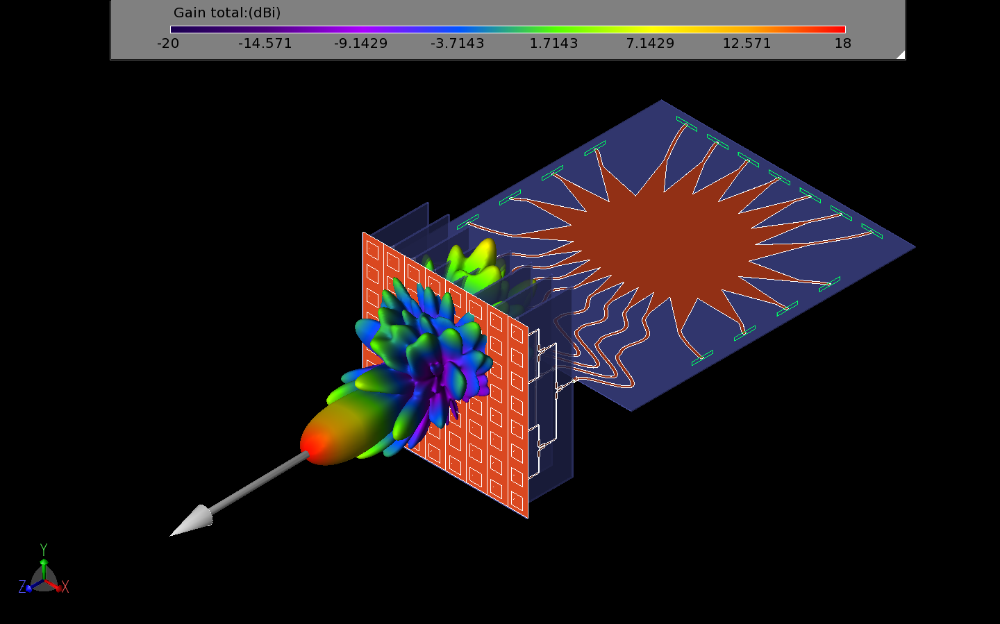
Figure 22: Shown in this figure is a three-dimension view of the beam pattern from input port 4 of the Rotman lens generated by the entire system.
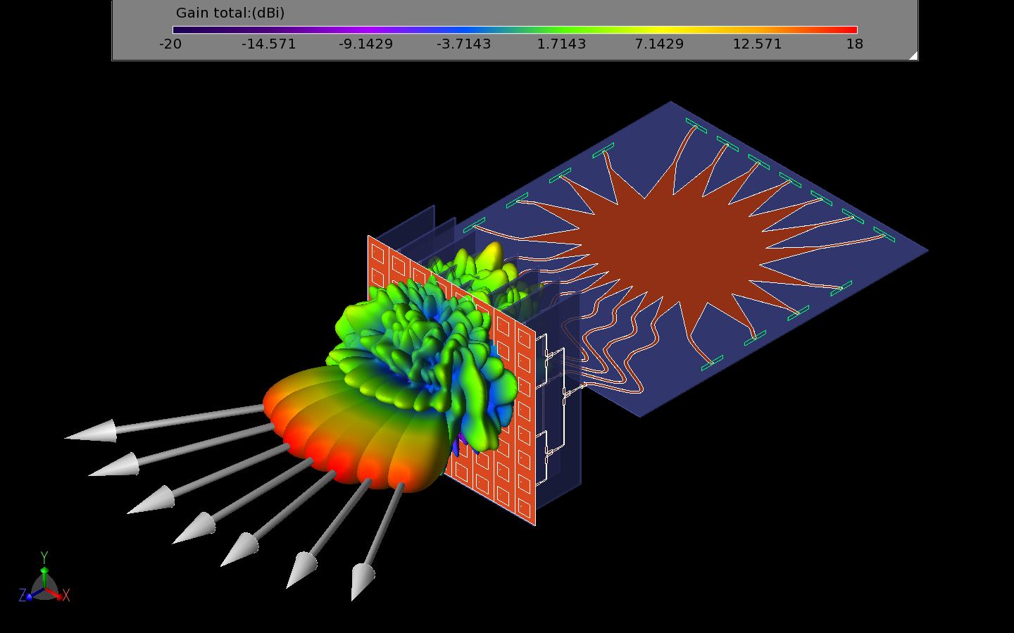
Figure 23: This figure shows all seven beams of the entire system as three-dimensional gain patterns.
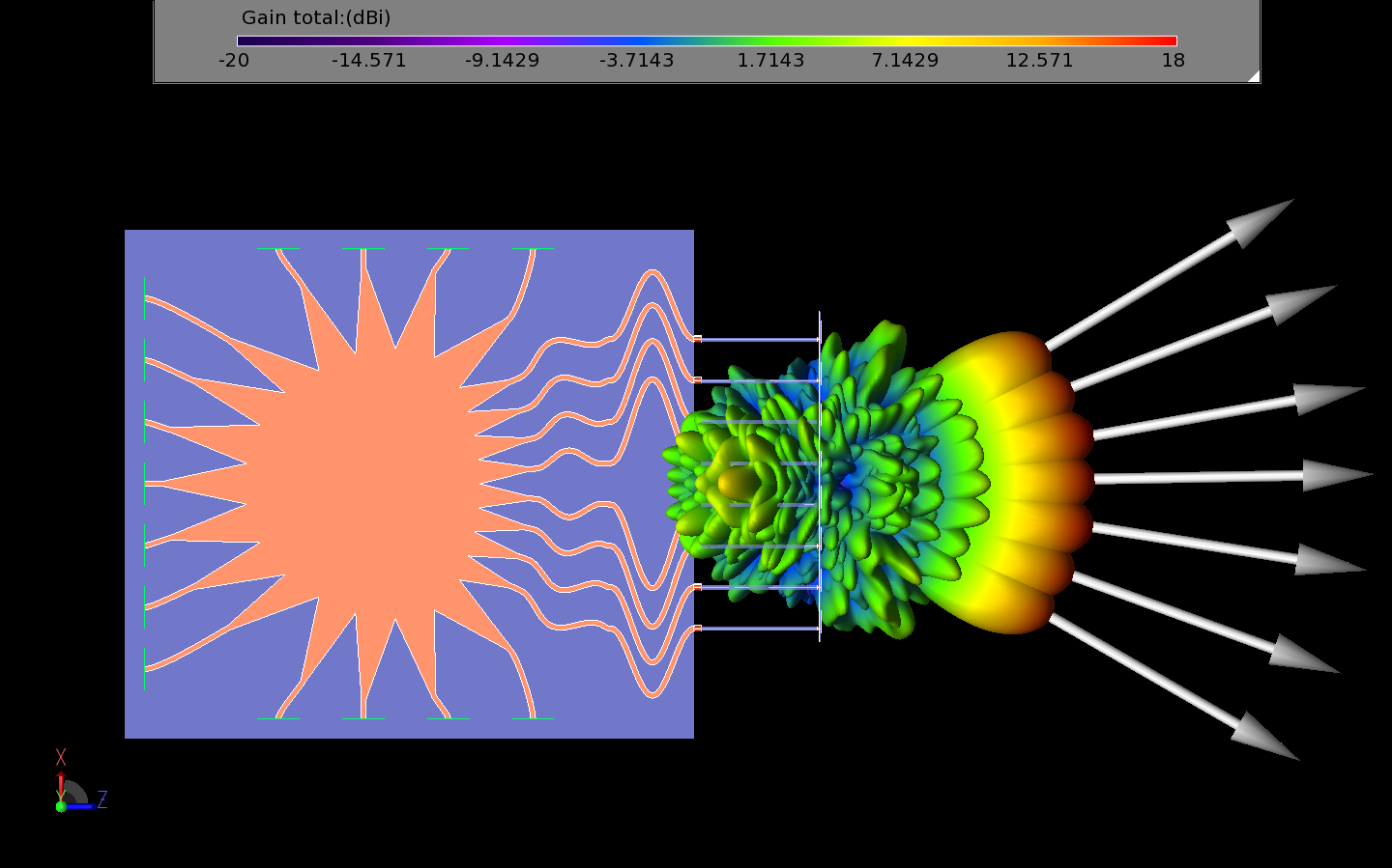
Figure 24: The seven beams generated by each input port of the Rotman lens are shown in three dimensions from a top view.
The visualization of the propagation of conduction currents on the device is a useful tool for ensuring that all connections between stages are good (no unconnected parts) and that the propagation speed to the arrays is the same. It is important for the transmission lines from the Rotman lens to the power dividers be the correct lengths to maintain the phase relationship of the wave front. In Figure 25, the current is seen propagating from the center beam port across the lens. By Figure 26 the current has just reached the output of the array ports and is entering the transmission lines. Figure 27 shows the current fully through the transmission lines and entering the power dividers. In Figure 28, the geometry display is disabled to better visualize the currents as they propagate through the first power divider stage and are still in good phase relation. Finally, in Figure 29 the currents have just reached the feeds of the patch antennas and are still in phase with each other.
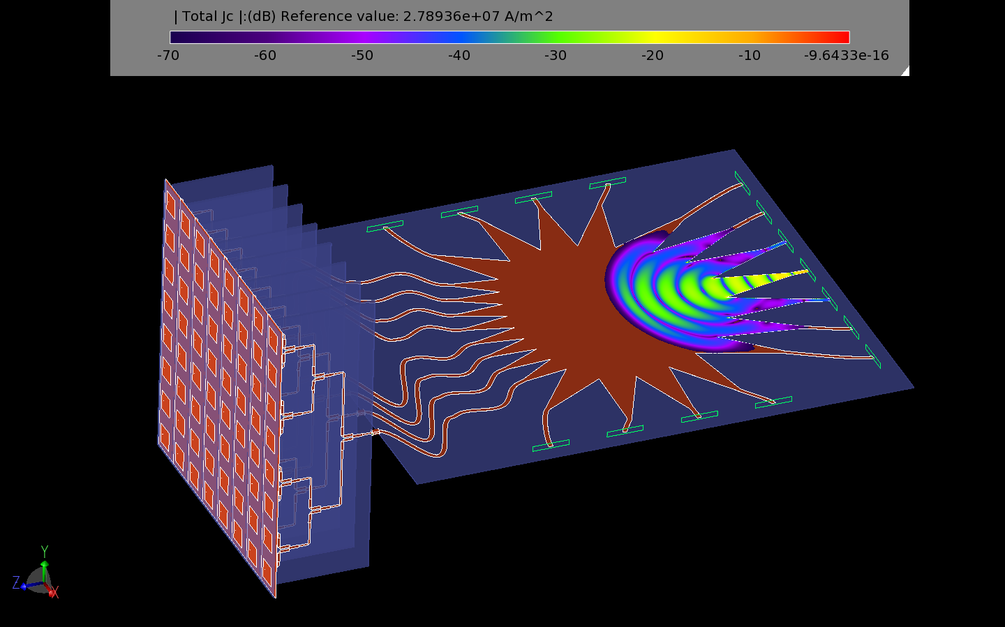
Figure 25: This figure shows the propagation of conduction currents from beam port 4 into the Rotman lens.
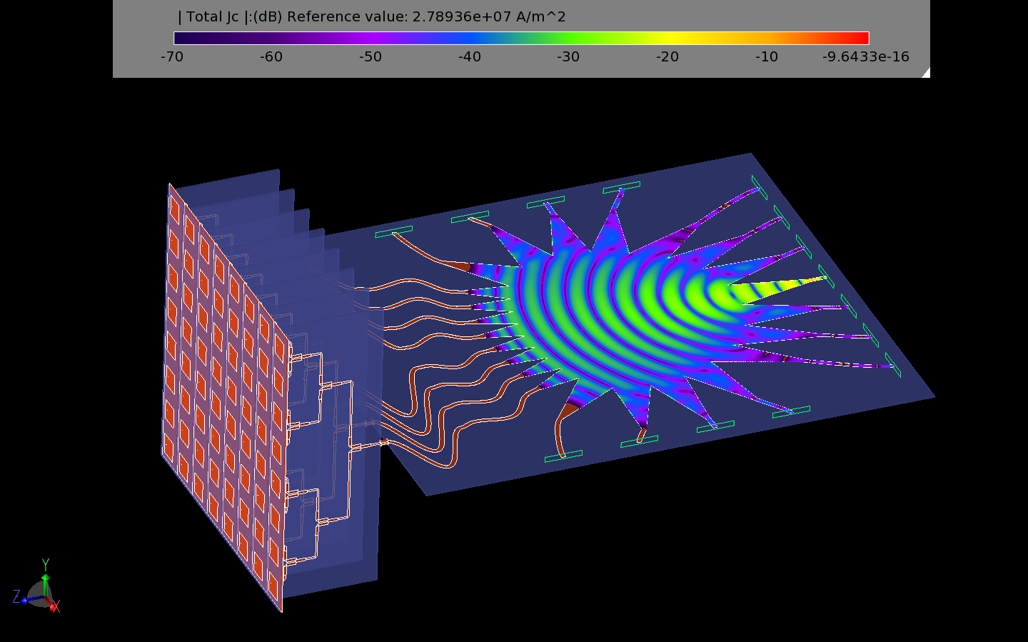
Figure 26: In this figure, the propagation of conduction currents from beam port 4 of the Rotman lens has just reached the array ports of the lens.
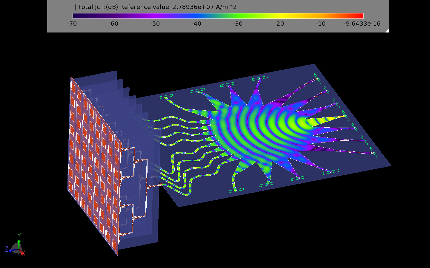
Figure 27: The propagation of the conduction currents has reached the ends of the array transmission lines and is entering the Wilkinson power divider elements. All currents appear to be in phase as they are arriving at the same location at the same time.
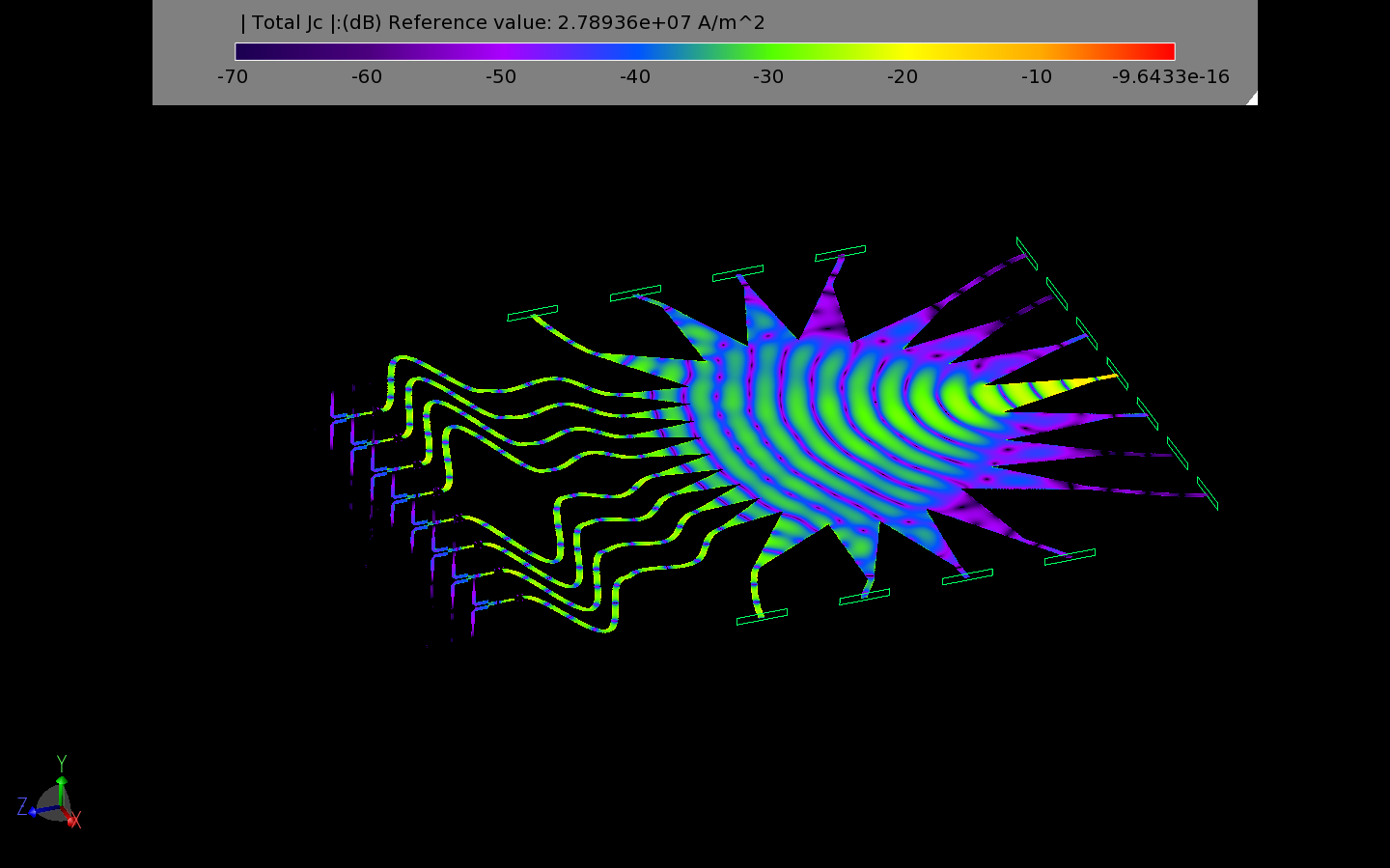
Figure 28: Here the display of the geometry has been disabled and only the conduction currents on the metal surfaces are shown. The fields are beginning to split in the first stage of the Wilkinson power divider.
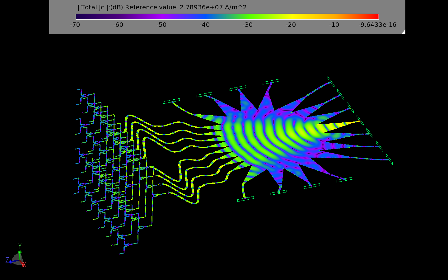
Figure 29: The currents have finally propagated across the entire structure and have reached the input ports of the antennas.
Summary
This example demonstrates one process for generating and analyzing a 28 GHz steerable array for 5G applications. Here the requirements were for beam coverage from -30 to 30 degrees in seven beams which was realized using a Rotman lens beamformer, eight 1 to 8 Wilkinson power dividers, and an 8x8 array of patch antennas.
For More Information:
If you would like to discuss how RLD and XFdtd can help your company with beamforming and antenna arrays, contact us today.


