In this example a cavity-backed slot/strip antenna is simulated in XFdtd using the XACT meshing feature. The simulated results for return loss, axial ratio, and gain are compared to measured results. The antenna design and measured results are taken from [1].
A CAD representation of the antenna structure is shown in Figure 1. The cavity is air-filled with perfectly conducting walls. The slots and ground plane are also perfectly conducting. Under the slots lies a very thin dielectric substrate which adds a challenging aspect to this otherwise fairly simple geometry. With a standard staircased mesh, the thickness of the dielectic layer will need to be defined by several FDTD cells. This would require either using a very small mesh size or some other technique such as a variable gridding. With XACT, the mesh size can be larger, but it is important to still make sure each layer of the geometry with distinct features is defined. In this geometry, fixed points are added to the Z plane of the slots and of the feed stub (top and bottom of the substrate) to ensure that each plane is defined. The base cell size is chosen as a much larger 0.8 mm cube, with a ratio allowing the smaller Z thickness to be defined. To aid in the simulation results, the outer surfaces of the dielectric substrate are covered by a thin averaging layer that has the dielectric value halfway between free space and the full dielectric value. Fixed points are also added to the end points of the feed to ensure they are properly connected between the feed line and the cavity wall. A view of the top layer of the antenna is shown in Figure 2 while the feed structure is shown in Figure 3.

Figure 1: A CAD representation of the cavity-backed antenna. The white material represents the metal layers while the green color is the dielectric substrate under the slots.
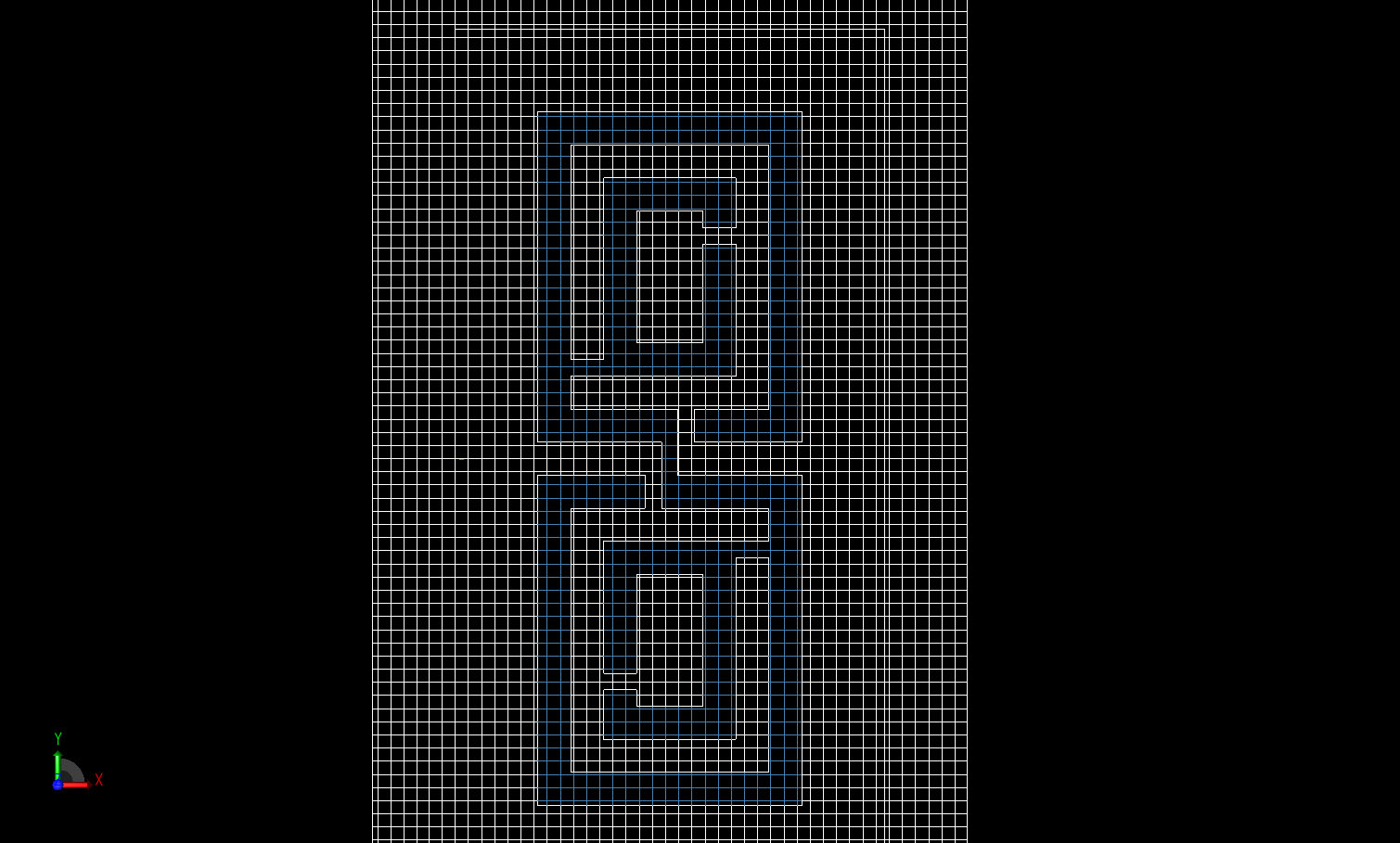
Figure 2: A two-dimensional cut of the XFdtd mesh of the antenna in the plane of the slots. Visible are the XACT-adjusted cells which perfectly conform to the edges of the CAD model.
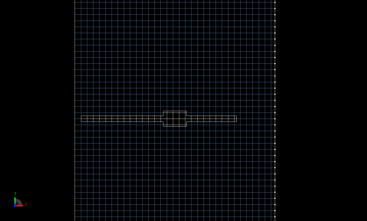
Figure 3: A two-dimensional view of the feed line shows the sub-cellular size of the microstrip line and the XACT mapping used to define the shape exactly.
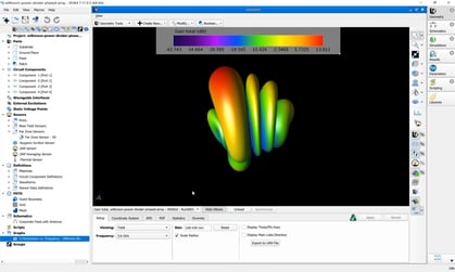
A frequency range of interest for the simulation is defined from 4 to 8 GHz. This automatically adjusts the waveform to cover this range of interest. The excitation for the actual antenna is provided by a coaxial line that attaches to the side of cavity and feeds the microstrip line on the bottom of the dielectric layer. A port is defined at the feed location, which is defined between the microstrip line and the cavity wall, much like the coaxial feed for the real antenna. Near zone fields are saved at this location for the computation of S-parameter results. Additionally, far zone sensors are defined to save the axial ratio and gain as a function of frequency directly above the antenna, and the gain in two principal planes through the center of the antenna. Antenna simulation is performed on a GPU cluster of four NVidia Telsa C870 GPU cards and takes 23 minutes. With a base cell size of 0.8 mm, the project required 611 thousand cells and 63 MB of memory. The S-parameter result for return loss at the feed compares well with the measured results defined in the paper (Figure 4). The axial ratio and gain results versus frequency also show good agreement when compared to the measured results (Figures 5 and 6). The circularly-polarized gain in the two principal planes is plotted for two different frequencies in Figures 7-10. The results are similar to those described in the paper.
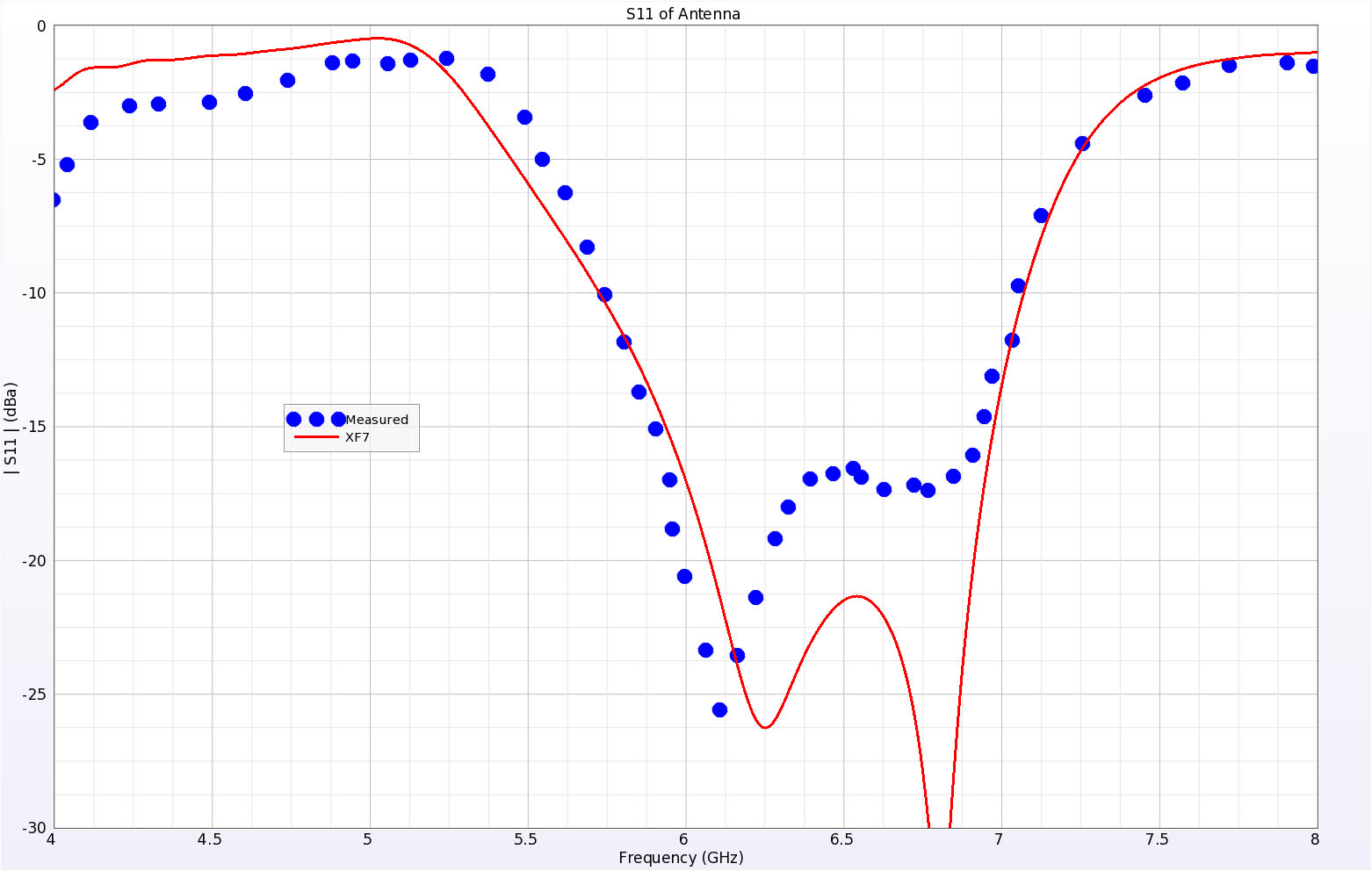
Figure 4: The simulated return loss from XFdtd7 is a good match to the measured data.
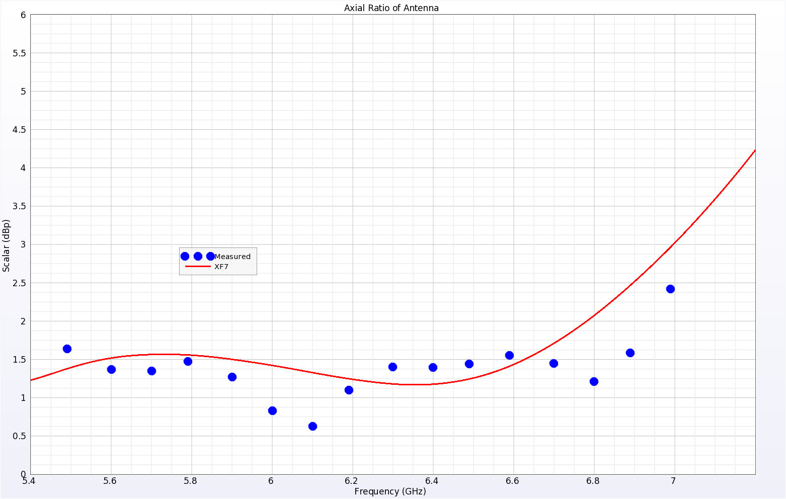
Figure 5: The axial ratio from the simulation and the measured data show similar results across the frequency range of interest.
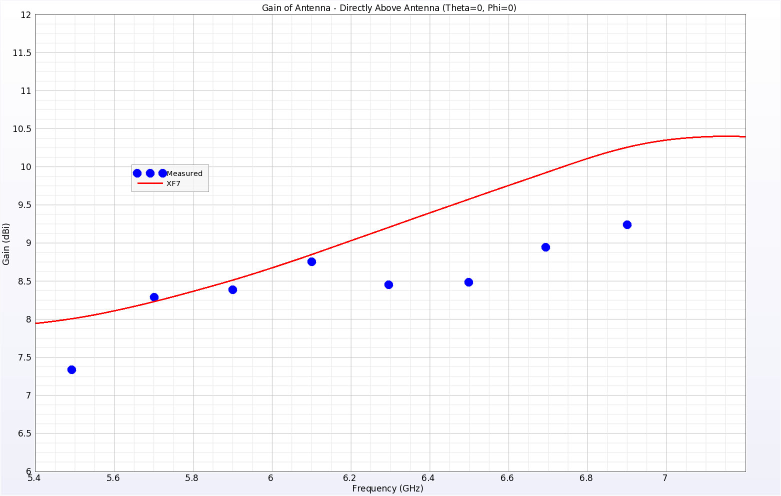
Figure 6: The gain of the simulated antenna at a point directly above the face of the antenna is a good match to the measured results.
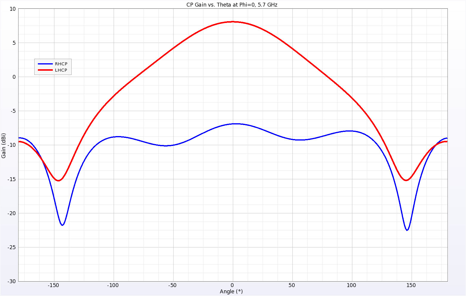
Figure 7: Here the right and left-hand circularly polarized gains are plotted in the Phi=0 plane (across the narrower width of the antenna) at 5.7 GHz.
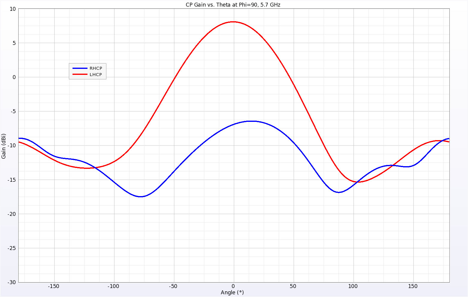
Figure 8: Here the right and left-hand circularly polarized gains are plotted in the Phi=90 plane (along the longer dimension of the antenna) at 5.7 GHz.
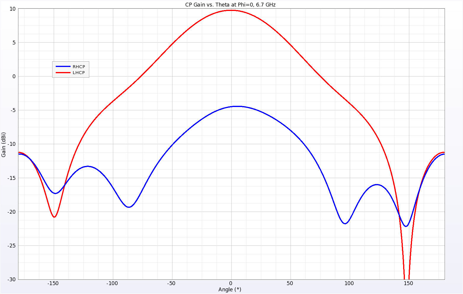
Figure 9: Here the right and left-hand circularly polarized gains are plotted in the Phi=0 plane (across the narrower width of the antenna) at 6.7 GHz.
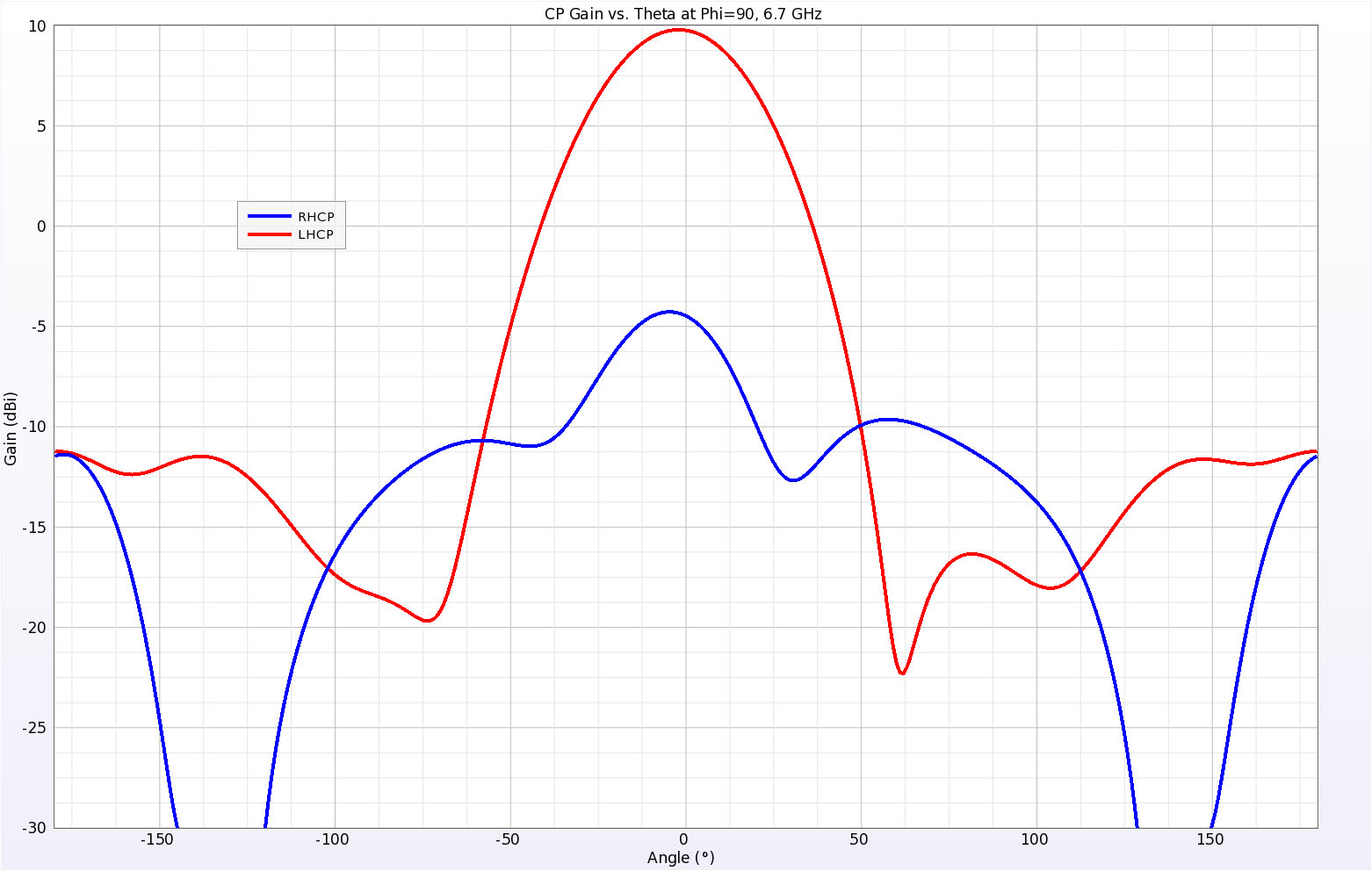
Figure 10: Here the right and left-hand circularly polarized gains are plotted in the Phi=90 plane (along the longer dimension of the antenna) at 6.7 GHz.
References
-
R. Li, B. Pan, A. N. Traille, J. Papapolymerou, J. Laskar, and M. M. Tentzeris, “Development of a Cavity-Based Broadband Circularly Polarized Slot/Strip Loop Antenna With a Simple Feeding Structure,” IEEE Trans. Antenna Propag., Vol. 56, No. 2, Feb. 2008, pp. 312-318.