Rotman Lens Designer (RLD) software is used to define and optimize a lens given a list of design parameters. The lens will have the following characteristics:
-
50 Ohm system impedance
-
Microstrip Design
-
Center frequency of 16 GHz, 4 GHz Bandwidth
-
20 degree Maximum Scan Angle
-
Half-wavelength element spacing
-
7 Beam ports
-
16 Array ports
-
All other parameters up to the designer
Entering the required parameters
On the physical properties tab of RLD, the system impedance and lens type may be set in the top two entry fields.
On the electrical properties tab of RLD, the center frequency, bandwidth and element spacing may be entered on the first three entry fields. In the middle of the tab the number of beams and array elements may be entered as well.
At this point, the rest of the design is up to the user. For the sake of comparison, two different designs will be considered.
Design 1
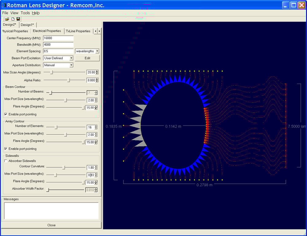
Design 1 uses a circular focal contour shape with a focal length set to 0.15 meter. The substrate is a dielectric with a permittivity of 2.33, a loss tangent of 0.0005 and a thickness of 0.508 mm. All other values on the physical properties tab are left at the default values. The focal length will be adjusted during the tuning process later.
For electrical properties of the lens, the aperture distribution is set to manual and the alpha ratio at 0.8. The flare angles for both the beam and array ports are set to 12 degrees with a maximum port size of 2 wavelengths. Port pointing is enabled for both the beam and array ports. Dummy ports will be used with a maximum port size of 1.15 wavelengths, a flare angle of 12 degrees, and a contour curvature of 1.20. The design at this untuned stage is shown in Figure 1.
With the center port active (port 4) and all other ports off, the array factor is plotted for the design. With the array factor plot displayed, the focal ratio slider is moved until a well-defined center beam is found (Figure 2). This occurs at a focal ratio of 1.0385. The beam to array phase error for this design can be found to be less than 0.5 degrees for all ports (Figure 3). With only beam 1 active, the array factor is still well-defined (Figure 4) with the beam offset to 16 degrees (80% of maximum scan angle as defined by the alpha ratio). The resulting design 1 prototype is shown in Figure 5.
Design 1 was then analyzed in the full wave, XFdtd solver. See the Rotman Lens with Linear Antenna Array example for a comparison of output from RLD and XF.
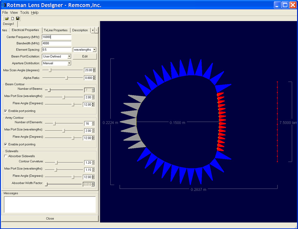
Figure 1: Untuned lens for Design 1 after most parameters are entered.
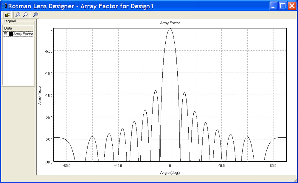
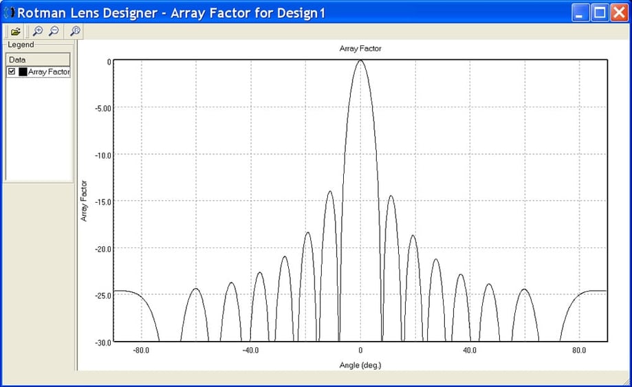
Figure 2: Array factor for Design 1 after tuning the focal ratio to a desired value.
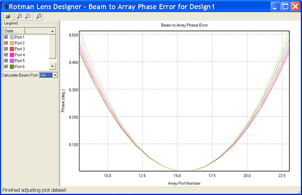
Figure 3: Phase error for tuned Design 1.
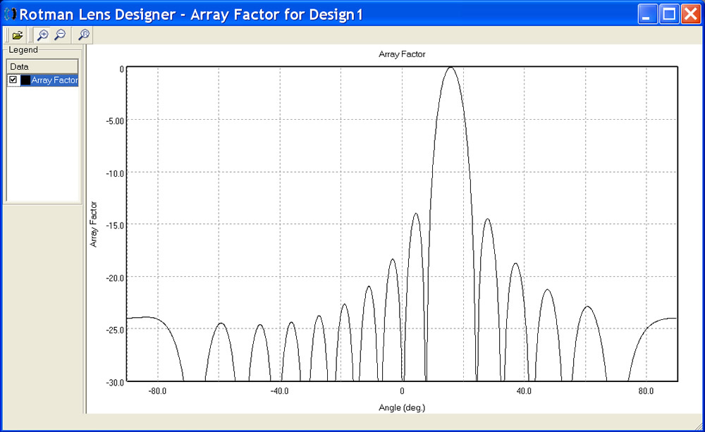
Figure 4: Array factor for Beam 1 of Design 1 showing scan angle offset.
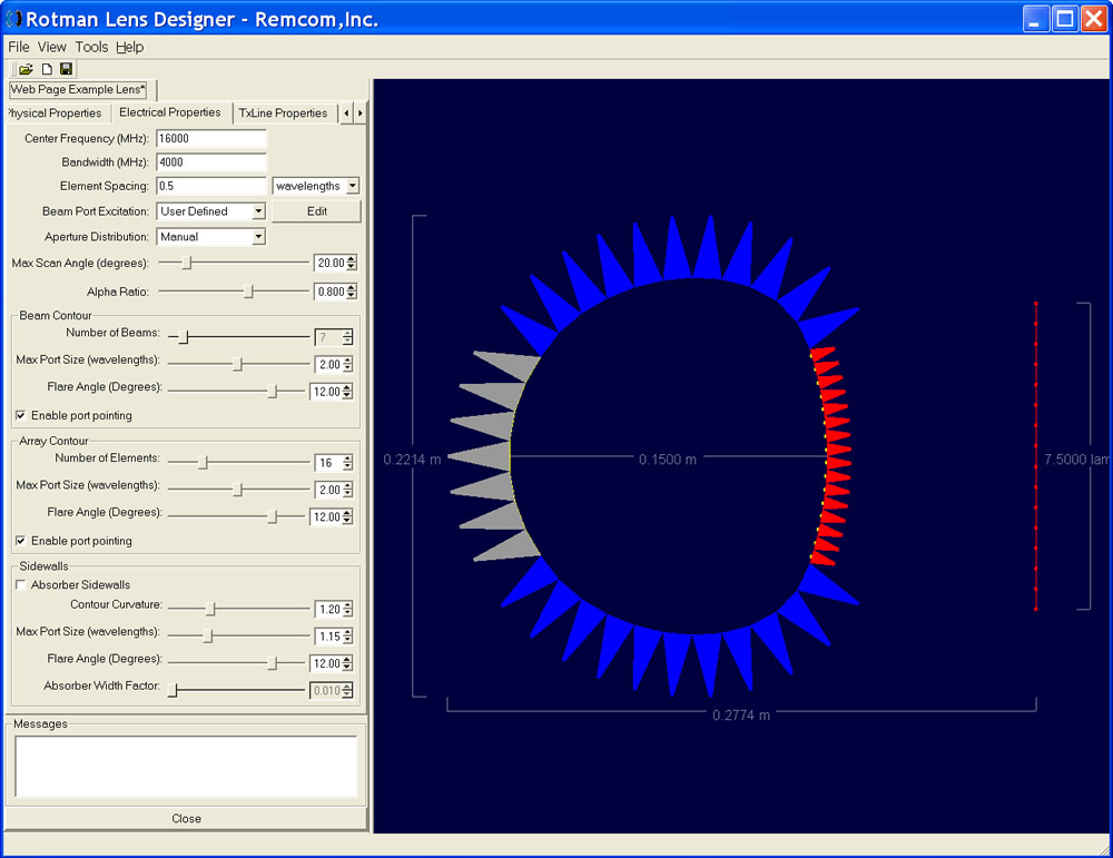
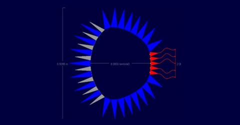
Figure 5: Tuned lens for Design 1.
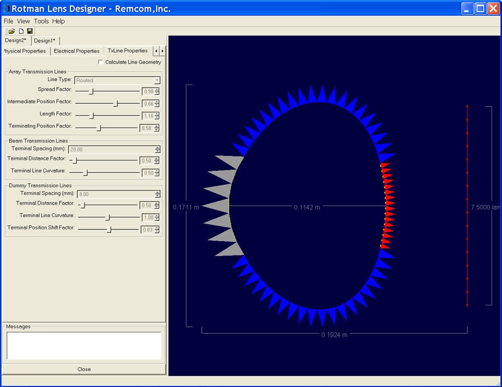
Figure 6: Tuned lens for Design 2.
Design 2
The second design will use the auto focal length setting and a dielectric with a permittivity of 6.15, a loss tangent of 0.0027, and with a thickness of 0.127 mm. The flare angles of all ports are set to 15 degrees. Also, the contour curvature is increased to 1.8 and the dummy port size is set to 0.93 wavelengths. Despite the changes, the lens is still tuned at a focal ratio of 1.0385 and the array factor is identical. The tuned design 2 is shown in Figure 6.
These two lens designs appear to perform identically according to the computed values. The major difference between them will be in the microstrip transmission lines that connect the ports to terminations. With design 1, the dielectric values yield thicker lines for the 50 ohm impedance, as shown in Figure 7. In contrast, design 2, shown in Figure 8 requires much thinner transmission lines.
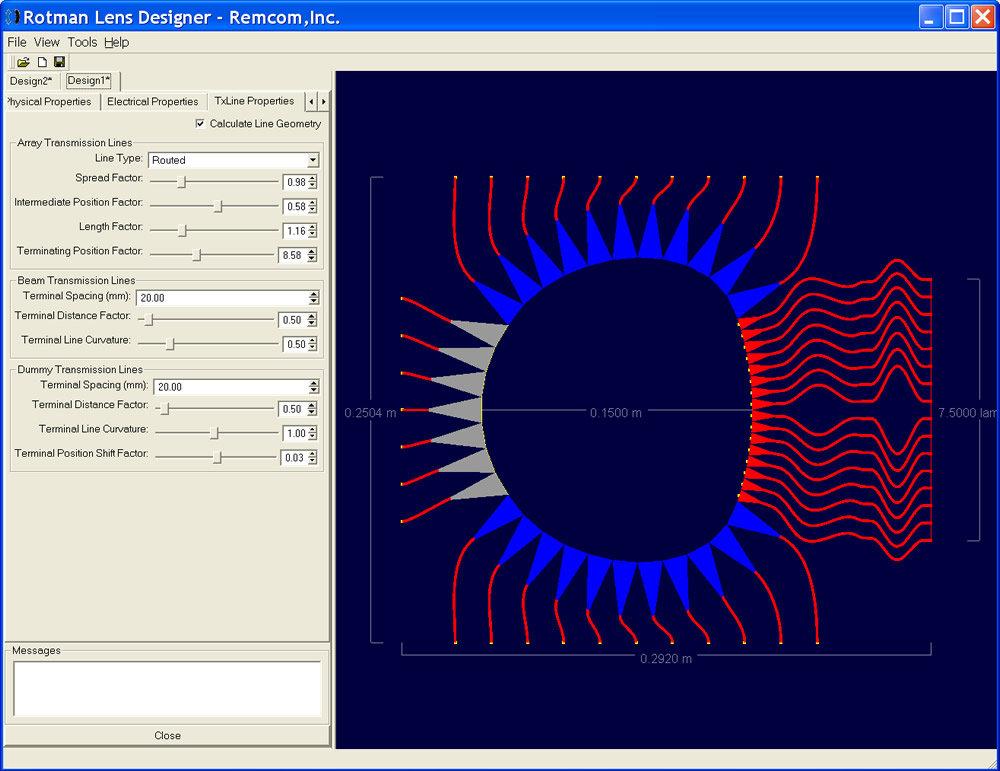
Figure 7: Thick transmission lines for tuned Design 1.