Impact of Substrate Thickness on Rotman Lens Designs
The Rotman Lens Designer (RLD) software is a first-level tool for designing microstrip and stripline Rotman Lenses. The calculations in the tool are based on Geometrical Optics combined with the lens design equations developed by Rotman [1] and others [2]. The RLD software can rapidly produce a tuned lens design from a set of design parameters. Many effects are approximated in the software, including the propagation of signals on the transmission lines, and the performance of an actual fabricated device might be different. In this example the thickness of the dielectric substrate is examined to show how certain thicknesses can lead to difficult design issues.
A general set of lens design parameters are selected for the example. The lens has a center frequency of 9.6 GHz and a bandwidth of 1.6 GHz. The scan angle is 40 degrees with output element spacing of 0.46431 wavelengths (separation distance between the output array elements). The lens is constructed as a microstrip with a substrate material that will vary in thickness over the range of available options described on the manufacturer's data sheet. The substrate will maintain a dielectric constant of 3.0 but will have thicknesses of 0.127 mm, 0.254 mm, 0.508 mm, 0.768 mm, and 1.524 mm. The number of beam and array ports will be fixed at 8 input and 8 output for all cases. In addition, for all cases the lens is tuned for good performance in the RLD software.
Figure 1 shows a basic 8x8 lens created by RLD with the beam ports to the left and the array ports to the right. On the top and bottom are dummy ports attached to the sidewalls that are intended to absorb any fields that strike them. The beam ports are numbered 1 to 8 from bottom to top. When the bottom port (Beam 1) is active, it will produce a beam centered at the positive maximum scan angle. A beam near the center, for example Beam 4, will produce a beam that is closer to broadside of the array. The top port (Beam 8) will produce a beam at the negative maximum scan angle. Figure 2 shows the 8 beams produced by the lens of Figure 1 with Beam 1 at the far right and Beam 8 at the far left.
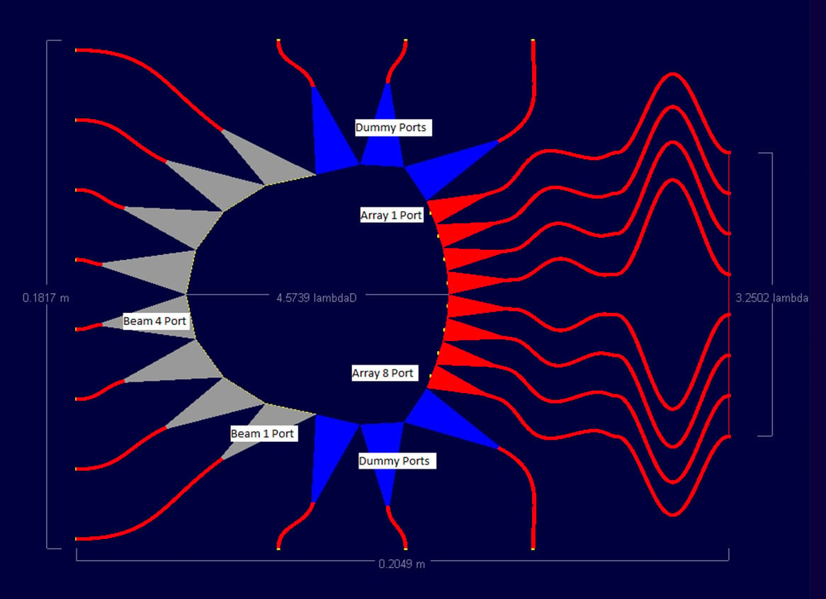
Figure 1: Shown is a basic microstrip lens generated in the RLD software. To the left are the beam (input) ports and to the right are the array (output ports). The port numbering is identified in the figure. The blue ports at the top and bottom are the dummy ports on the sidewalls. This example will vary the curvature of the sidewall while holding other lens parameters fixed.
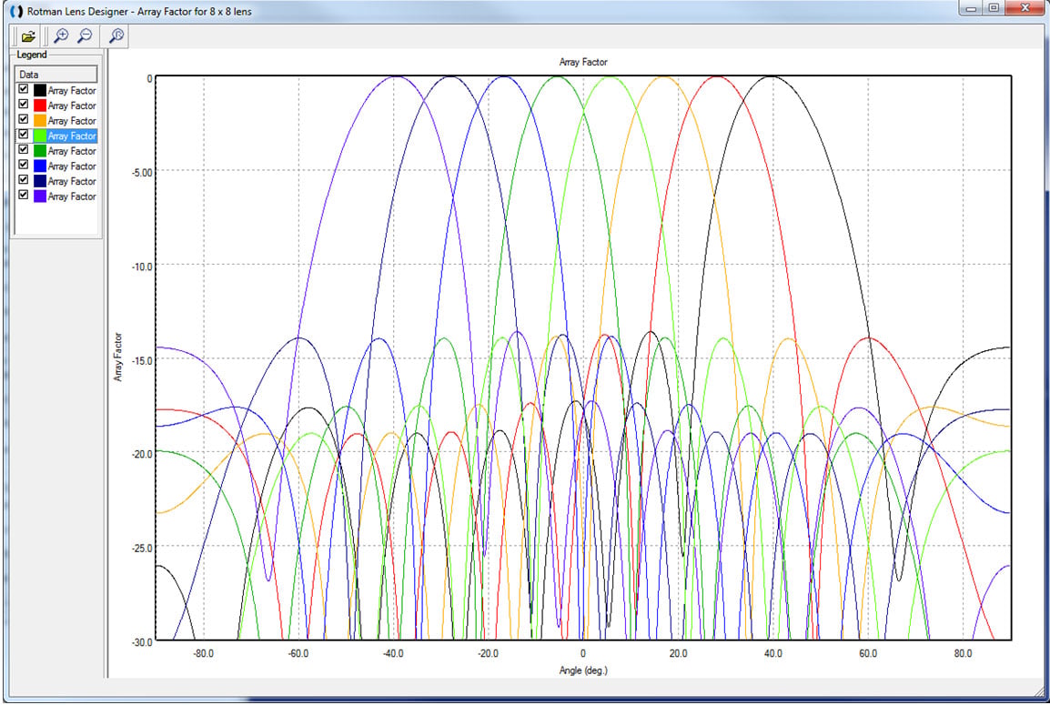
Figure 2: This is a plot of the 8 beams produced by the lens of Figure 1 in the RLD software. The maximum scan angle of the beam is +/- 40 degrees which is generated by ports 1 and 8 on the input side.
The first lens simulated will have the thinnest substrate of 0.127 mm and shown in Figure 3 where it can be seen that the transmission lines to the ports are very thin relative to the rest of the lens design. When simulated in XFdtd, the small width of the transmission lines requires a fairly high resolution model of the geometry resulting in large memory needs and significant simulation times. Figure 4 shows the pattern for Beam 1 of the lens comparing RLD results with those from XFdtd. As can be seen in Figure 4, the correlation is moderate (around 80%) with a slightly shifted main beam and some variation in the side lobes. For the near-center Beam 4 pattern shown in Figure 5, the correlation is better with just some variation in some of the side lobes.
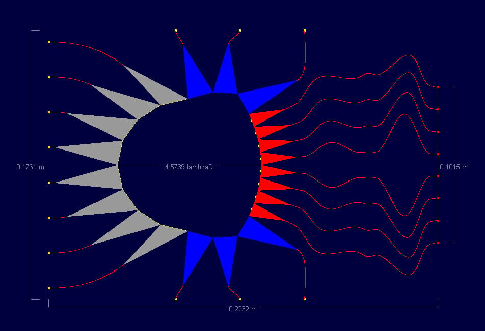
Figure 3: Shown is the Rotman lens as designed on a 0.127 mm substrate. Note the very thin transmission lines
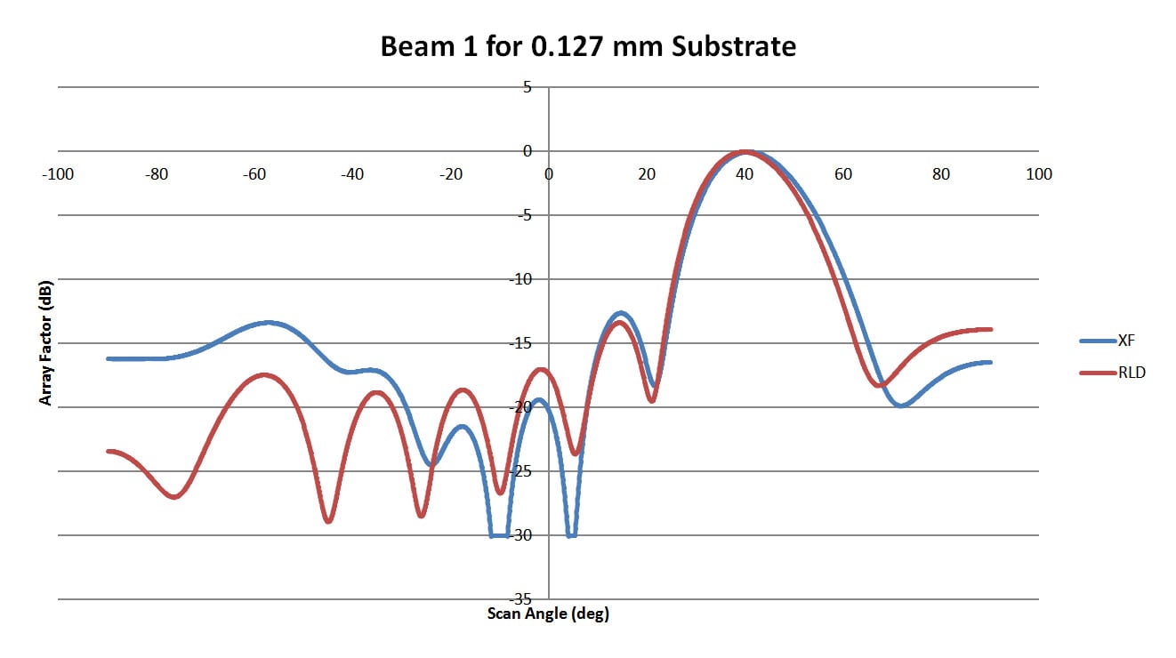
Figure 4: This plot shows the pattern for Beam 1 of the 0.127 mm substrate lens of Figure 3. The correlation between RLD and XFdtd is moderate.
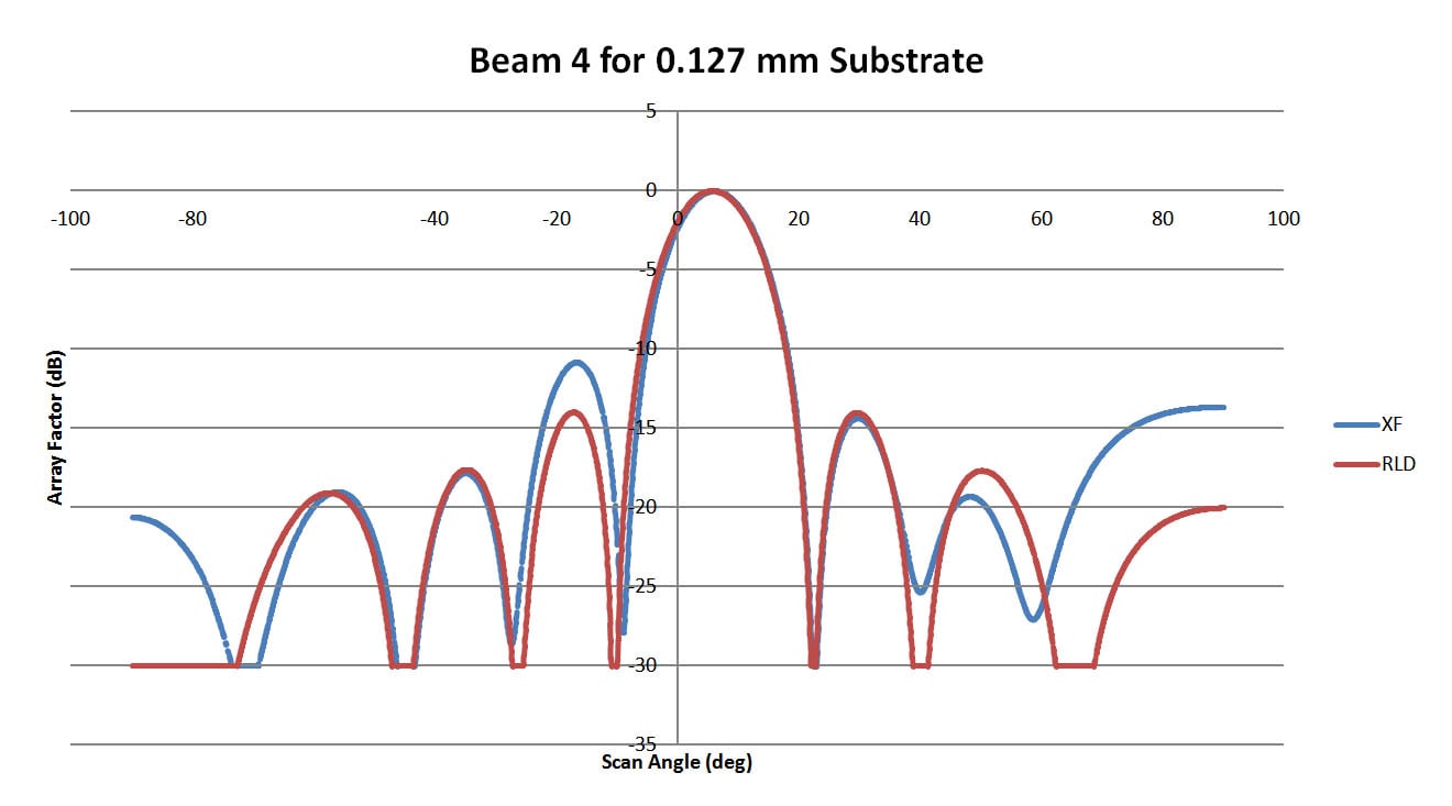
Figure 5: This plot shows the pattern for Beam 4 of the 0.127 mm substrate lens of Figure 3. The correlation with XFdtd is higher for this lens although there is some variation in the side lobes.
Increasing the substrate thickness to 0.254 mm makes a dramatic change in the lens and the performance. The lens, shown in Figure 6, can be seen to be quite similar to that of the 0.127 mm thick substrate shown in Figure 3, but with slightly thicker transmission lines. The beam patterns show very high correlation between RLD and XFdtd as well, as can be seen in Figures 7 and 8. Similar results are obtained for the lenses with 0.254 mm and 0.768 mm thick substrates.
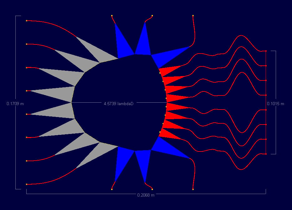
Figure 6: Shown is the Rotman lens as designed on a 0.254 mm substrate. The lenses designed on 0.508 mm and 0.768 mm substrates are similar and give similar performance.
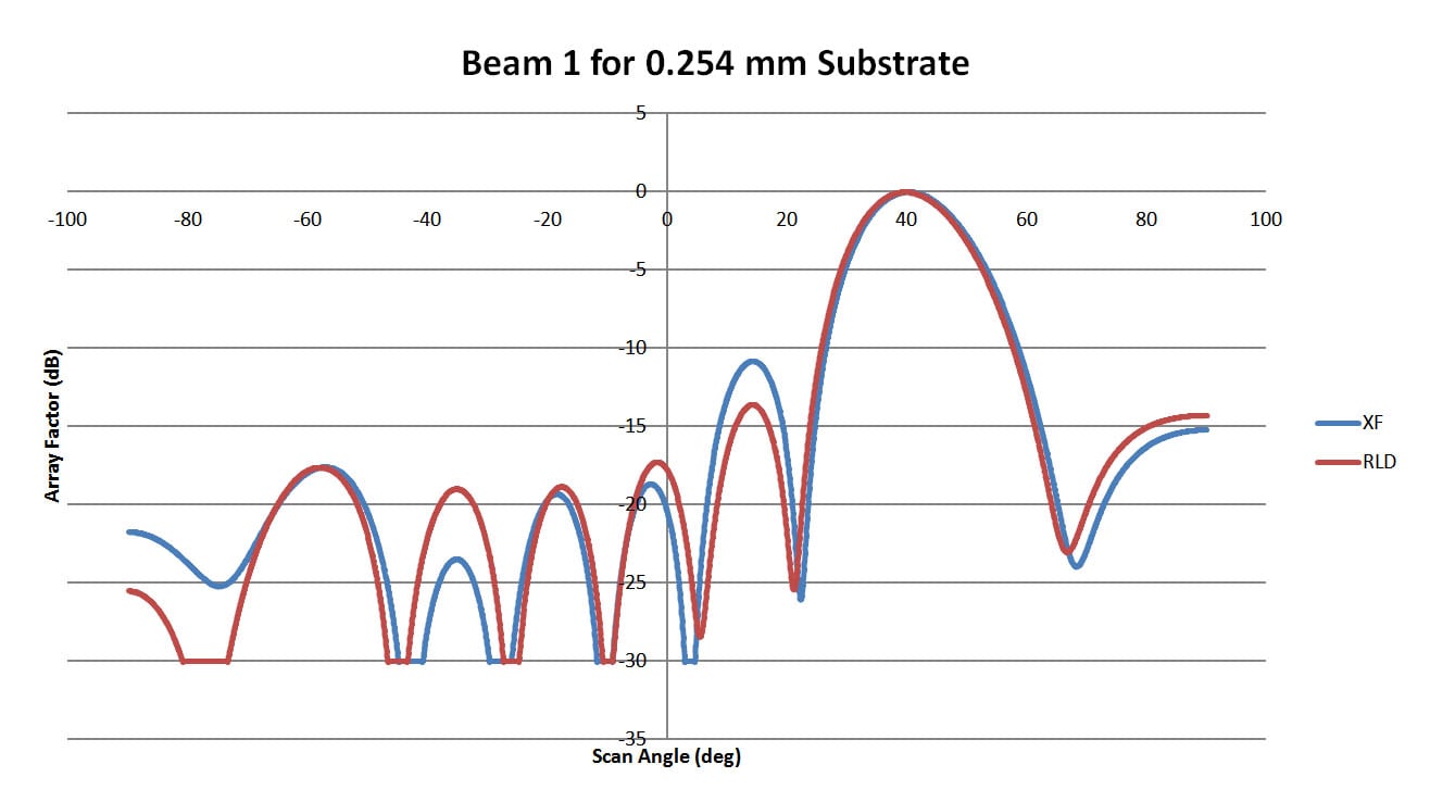
Figure 7: This plot shows the pattern for Beam 1 of the 0.254 mm substrate lens of Figure 6. The correlation with XFdtd is high.
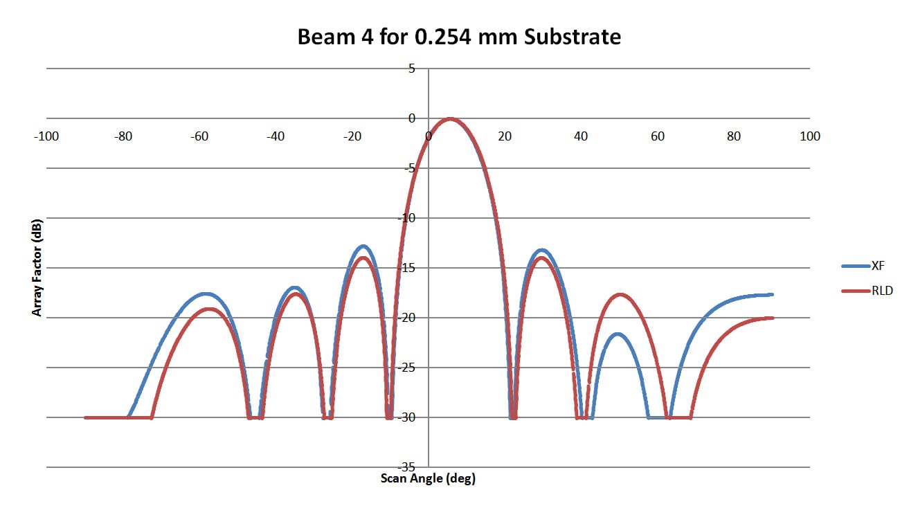
Figure 8: This plot shows the pattern for Beam 4 of the 0.254 mm substrate lens of Figure 6. The correlation with XFdtd is high.
Finally, for the 1.524 mm thick substrate, the transmission lines become quite wide which introduces some difficulty with the layout of the lines and requires the lines to be much longer in order to resolve the various bends in the line while maintaining the proper length ratios between lines. The geometry is shown in Figure 9 using a layout similar to that used for the thinner substrate lenses. This lens design does not yield well-correlated results between RLD and XFdtd which indicates that the transmission lines are introducing errors. A modified design with extended array transmission lines and modified dummy ports on the sidewalls, shown in Figure 10, gives much better performance with high correlation between RLD and XFdtd, as can be seen in Figures 11 and 12.
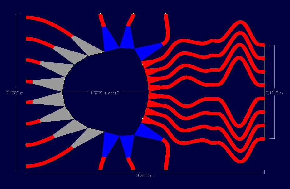
Figure 9: Shown is the original design of the Rotman lens on a 1.524 mm substrate. This lens performed poorly in XFdtd indicating that there was some error introduced in the transmission lines.
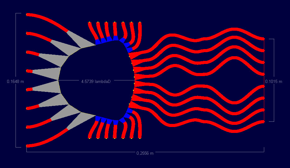
Figure 10: Shown is the revised design of the Rotman lens on a 1.524 mm substrate. This lens has smaller dummy ports which aided in the lens layout and has longer array transmission lines that allow for a better layout of the lines
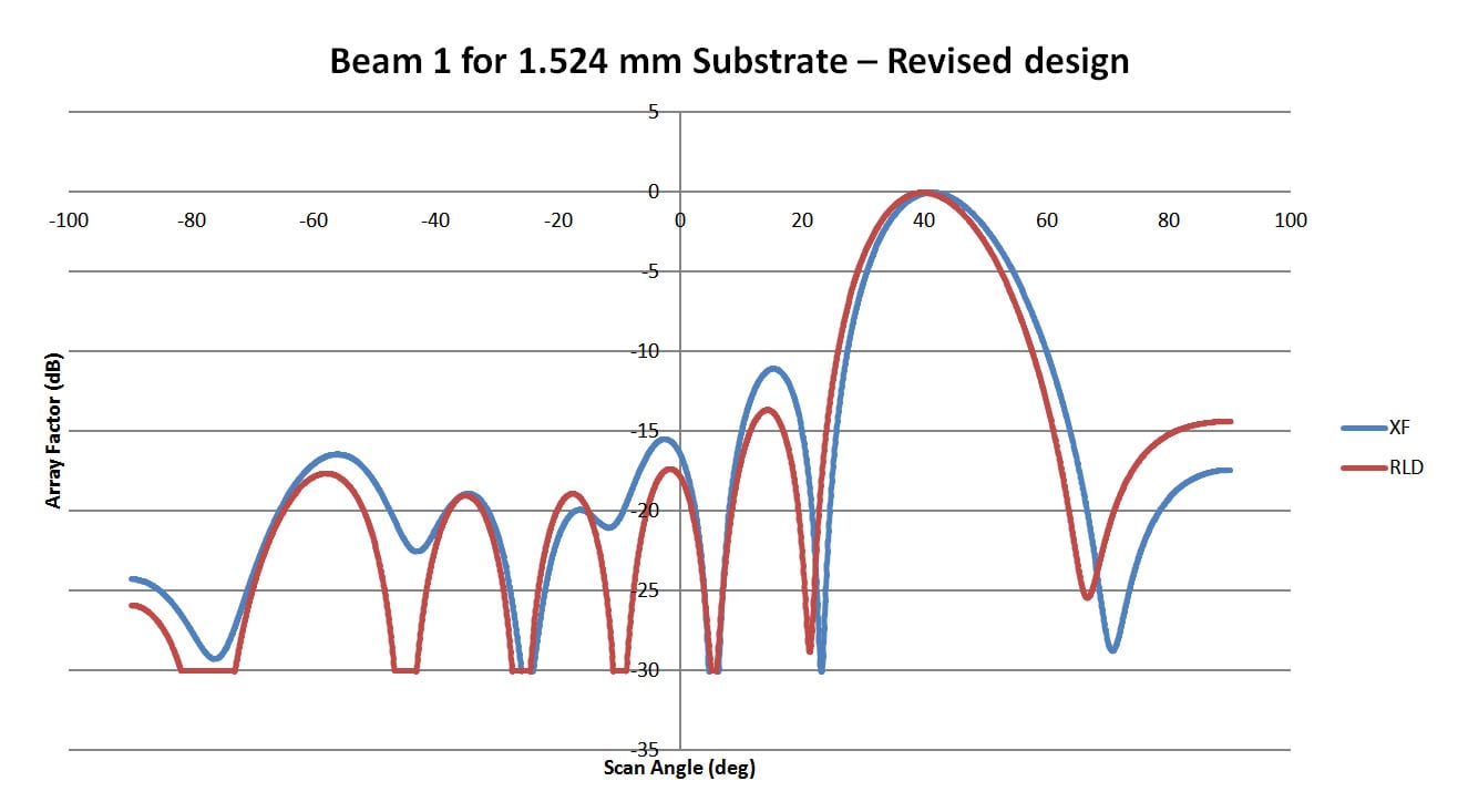
Figure 11: This plot shows the pattern for Beam 1 of the 1.524 mm substrate lens of Figure 10. The correlation with XFdtd is about 90% although there is a slight shift of the main beam.
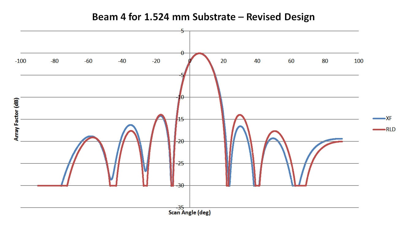
Figure 12: This plot shows the pattern for Beam 4 of the 1.524 mm substrate lens of Figure 10. The correlation with XFdtd is about 90%.
Conclusion
This example demonstrates the impact of differing substrate thicknesses on the lens layout and highlights the issues that can arise when a too-thin or too-thick substrate is chosen. The RLD software gives similar results for the beam patterns for all lenses because it does not fully evaluate the transmission of the fields along the transmission lines. Simulations with XFdtd are more rigorous and show the impact of errors introduced by poor line layout. In this particular study it was found that a substrate that produces a transmission line with a width 1-2% of the lens width produces best results as determined by correlation between RLD and XFdtd results. This is a general rule that can be applied to other designs but is not rigorously determined.
Reference
-
Rotman, W. and R. Turner, "Wide-Angle Microwave Lens for Line Source Applications," IEEE Transactions on Antennas and Propagation, vol. 11, no. 6, pp. 623-632, Nov. 1963.
-
Hansen, R. C., "Design Trades for Rotman Lenses," IEEE Transactions on Antennas and Propagation, vol. 39, no. 4, pp. 464-472, April 1991.
Request Project Files
Thank you for your interest in this application example. Please complete the form below to download the Impact of Substrate Thickness on Rotman Lens Designs project files.
