Matching Network Simulation and Design Resources
-

Webinars
Overview of XFdtd's Schematic Editor and Optimization for Matching Network Design
This webinar demonstrates the full range of features available to users, with a focus on recent updates that include optimization of component values, impedance and aperture tuners with tune codes, and system efficiency results.
Explore Resource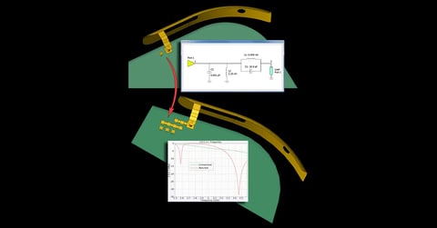
Webinars
Antenna Design Workflow Using Full-Wave Matching Circuit Optimization
The design of a matched antenna is a fairly involved process. This webinar shows how XFdtd simplifies this process by providing tools to parameterize the unmatched antenna, determine S11, synthesize a matching network topology with Optenni Lab, and determine the final component values using the Circuit Element Optimizer.
Explore Resource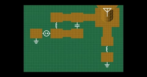
Webinars
Introduction to XFdtd’s Circuit Element Optimizer
Remcom’s Circuit Element Optimizer for XFdtd is a unique tool for full wave matching circuit optimization. This webinar introduces the capability and provides an example of how it is used. A GPS/Bluetooth antenna and an LTE antenna are used for the demonstration.
Explore Resource -

Application Examples
FDTD Simulation: Optimizing an LTE Antenna's Matching Network
A simple antenna for LTE band operation is added to the PC board of a smartphone in XFdtd and the matching circuit is tuned for operation in multiple frequency bands. The component values in the matching network are chosen to maximize system efficiency.
Explore Resource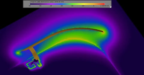
Application Examples
Full Wave Simulation: Matching Network Design for GPS / Bluetooth Antenna
XFdtd's Circuit Element Optimizer is used to determine optimal matching component values for a dual purpose antenna.
Explore Resource -
Videos
Impedance Tuner Matching in XFdtd
This presentation will demonstrate the advantages of using XFdtd for complex matching network design.
Explore Resource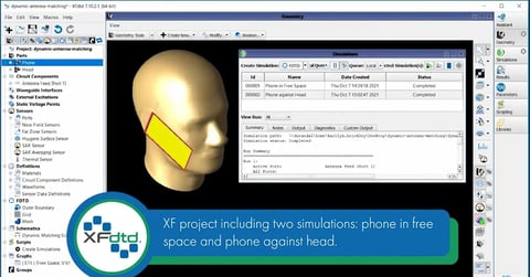
Videos
Dynamic Matched Antenna Using XFdtd’s Schematic Editor
In this video tutorial, an antenna's intrinsic impedance is simulated for two conditions--in free space and against a head. A three-port switch with two possible states is also included.
Explore Resource2.webp?width=480&height=251&name=maxresdefault%20(2)2.webp)
Videos
Tune a Tunable Matched Antenna Using XFdtd’s Schematic Editor
In this tutorial, we demonstrate the ease of adjusting or tuning, multiple operating modes so that capacitance values match various frequency bands. Using XF’s schematic editor with tuning slider bars, the correct values can be found in moments.
Explore Resource -

Publications
What’s New in XFdtd®
XFdtd Release 7.11.1 introduces several enhancements designed to elevate simulation accuracy, expand analysis capabilities, and streamline the engineering workflow. This release reflects Remcom’s continued focus on solving high-value challenges in antenna design, PCB modeling, and phased array system development.
Explore Resource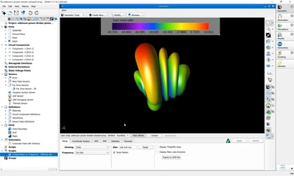
Publications
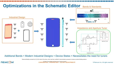
Mastering XFdtd’s Schematic Editor: A Comprehensive Overview
Dive into the capabilities of XFdtd’s schematic editor and discover how it transforms schematic creation, analysis, and optimization in engineering.
Explore Resource
Publications
Full Wave Matching Circuit Optimization Shortens Design Iterations
Full wave matching circuit optimization (FW-MCO) is a new technology that combines full wave, 3D EM simulation with circuit optimization into a novel approach for solving an age-old RF problem: determining which component values provide the desired match for a given matching network layout. This article describes the design process using the design of a matching circuit for a GPS-Bluetooth antenna.
Explore Resource
Save time and reduce costs.
Contact Remcom today for a customized solution to your most complex electromagnetic challenges.
Request a Quote